Intel Announces first 22nm 3D Tri-Gate Transistors, Shipping in 2H 2011
by Anand Lal Shimpi on May 4, 2011 2:05 PM ESTEarlier this week Intel sent us a cryptic message:
I wanted to invite you to an Intel press conference on Wednesday May 4th at 9:30am Pacific time. Intel will be making its most significant technology announcement of the year. No further details will be provided in advance. The event will be held in San Francisco so for those of you are local in the SF Bay Area please attend in person if you like. It will also webcasted live. Tune-in details and logistics are below. Please let me know if you can attend.
A while ago Intel decided that a nice way to drive up its stock price would be to behave more like Apple, keeping major announcements under wraps and introducing them on its own terms to hopefully build up anticipation and excitement for Intel's announcements. You've seen examples of this with how closely Intel held Sandy Bridge's architectural details before its presentation at IDF, and how little we knew about Quick Sync (Sandy Bridge's hardware video transcoder) until Intel decided it was time to talk about it.
Apple can get away with it since most of its products are tangible, consumer facing devices. Intel's technologies are arguably even more important, but they're just not as easy for the general populace to get excited about. Today's announcement is the perfect example of just that.
Earlier today Intel announced that its 22nm process would not use conventional planar transistors but rather be the first time Intel is using 3D Tri-Gate transistors. This is a huge announcement that fuels Intel's leadership in the mobile/desktop/server CPU space and makes it a lot more attractive in the SoC space, let's understand why.
The Transistor
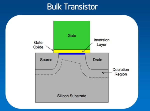
Here's a simple diagram of a standard 32nm planar transistor, exactly what you'd find in a Sandy Bridge CPU:
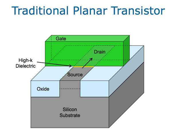
Image Courtesy Intel Corporation
I spent a couple of semesters as a computer engineering student a few years ago studying how these things work. There's a lot of math and it's not fun to do over and over again so we'll ignore all of that for now. The basics are thankfully much more fun to understand.
Image Courtesy Intel Corporation
The goal of a transistor is to act as a very high speed electrical switch. When on, current flows from the transistor's source to the drain. When off, current stops. The inversion layer (blue line above) is where the current flow actually happens.
Ideally a transistor needs to do three things:
1) Allow as much current to flow when it's on (active current)
2) Allow as little current to flow when it's off (leakage current)
3) Switch between on and off states as quickly as possible (performance)
The first item impacts how much power your CPU uses when it's actively doing work, the second impacts how much power it draws when idle and the third influences clock speed.
In conventional planar transistors it turns out that voltage in the silicon substrate impacts leakage current in a negative way. Fully depleted SOI (silicon on insulator) is an option to combating this effect.
The smaller you make the transistors, the more difficult it is to make advancements in all three of these areas all while increasing transistor density. After all not only do you have to worry about keeping power under control, but the whole point to shrinking transistor dimensions is to cram more of them into the same physical die area, thus paving the way for better performance (more cores, larger caches, higher performance structures, more integration).
The 3D Tri-Gate Transistor
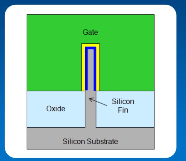
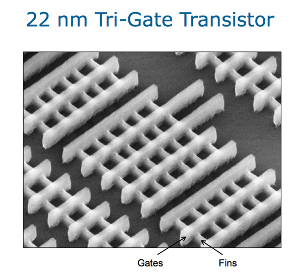
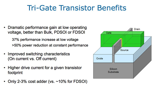
A 3D Tri-Gate transistor looks a lot like the planar transistor but with one fundamental change. Instead of having a planar inversion layer (where electrical current actually flows), Intel's 3D Tri-Gate transistor creates a three-sided silicon fin that the gate wraps around, creating an inversion layer with a much larger surface area.
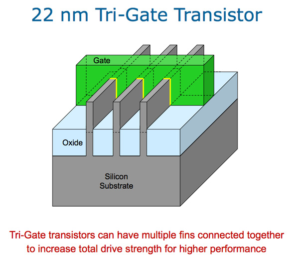
Image Courtesy Intel Corporation
There are five outcomes of this move:
1) The gate now exerts far more control over the flow of current through the transistor.
2) Silicon substrate voltage no longer impacts current when the transistor is off.
3) Thanks to larger inversion layer area, more current can flow when the transistor is on.
4) Transistor density isn't negatively impacted.
5) You can vary the number of fins to increase drive strength and performance.
The first two points in the list result in lower leakage current. When Intel's 22nm 3D Tri-Gate transistors are off, they'll burn less power than a hypothetical planar 22nm process.
Image Courtesy Intel Corporation
The third point is particularly exciting because it allows for better transistor performance as well as lower overall power. The benefits are staggering:
Image Courtesy Intel Corporation
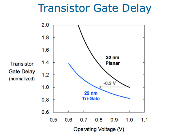
At the same switching speed, Intel's 22nm 3D Tri-Gate transistors can run at 75 - 80% of the operating voltage of Intel's 32nm transistors. This results in lower active power at the same frequency, or the same active power at a higher performance level. Intel claims that the reduction in active power can be more than 50% compared to its 32nm process.
Image Courtesy Intel Corporation
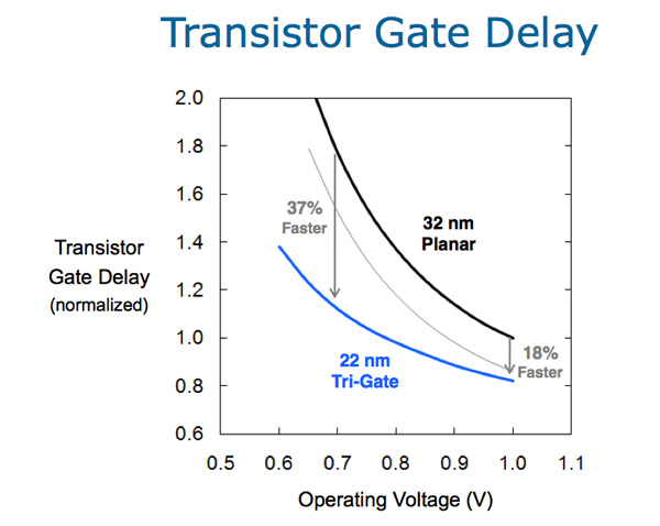
At lower voltages Intel is claiming a 37% increase in performance vs. its 32nm process and an 18% increase in performance at 1V. High end desktop and mobile parts fall into the latter category. Ivy Bridge is likely to see gains on the order of 18% vs. Sandy Bridge, however Intel may put those gains to use by reducing overall power consumption of the chip as well as pushing for higher frequencies. The other end of that curve is really for the ultra mobile chips, this should mean big news for the 22nm Atom which I'm guessing we'll see around 2013.
Image Courtesy Intel Corporation
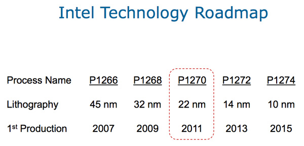
You'll note that the move to 3D Tri-Gate transistors doesn't negatively impact transistor density. In fact Intel is claiming a 2x density improvement from 32nm to 22nm (you can fit roughly twice as many transistors in the same die area at 22nm as you could on Intel's 32nm process).
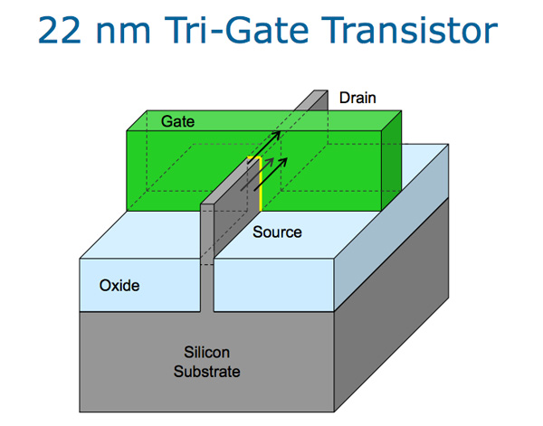
Image Courtesy Intel Corporation
It's also possible to vary the number of fins to impact drive strength and performance, allowing Intel to more finely tune/target its 22nm process to various products.
The impact on manufacturing cost is also minimal. Compared to a hypothetical Intel 22nm planar process, the 3D Tri-Gate process should only cost another 2 - 3%
Image Courtesy Intel Corporation
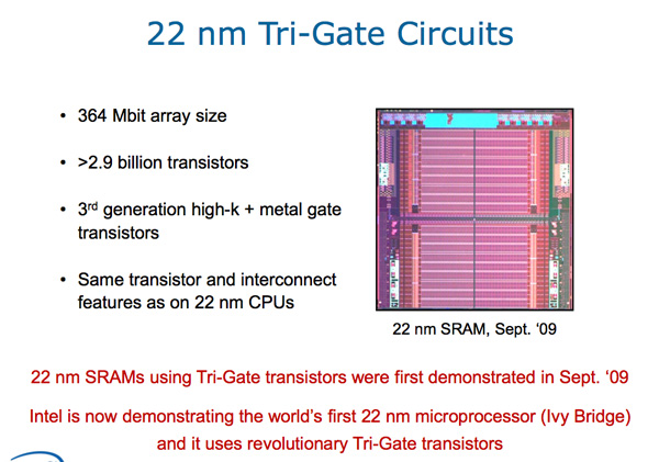
All 22nm products from Intel will use its 3D Tri-Gate transistors.
What Does This Mean
Intel's Ivy Bridge is currently scheduled for a debut in the first half of 2012. Intel is purposefully being vague about the release quarter as Sandy Bridge is doing well and isn't facing much competition at the high end at least.
The impact of Intel's 22nm 3D Tri-Gate transistors on high end x86 CPUs will be significant. Intel isn't expecting its competitors to move to a similar technology until 14nm. The increases in switching speed at the same voltage could allow Intel to finally hit or exceed that magical 4GHz barrier in a stock CPU. I suspect Intel will likely use the gains to deliver lower power CPUs however there's always the possibility of some very fast Extreme Edition parts.
Image Courtesy Intel Corporation.
The bigger story here actually has to do with Atom. The biggest gains Intel is showing are at very low voltages, exactly what will benefit ultra mobile SoCs. Atom has had a tough time getting into smartphones and while we may see limited success at 32nm, the real future is what happens at 22nm. Atom is due for a new microprocessor architecture in 2012, if Intel goes the risky route and combines it with its 22nm process it could have a knockout on its hands.




82 Comments
View All Comments
Akaz1976 - Wednesday, May 4, 2011 - link
If we wont see Atoms based ont his tech till 2013, does this mean that ARM camp would be able to come up with a similar solution by then? and thus retain its advantage?nitrousoxide - Wednesday, May 4, 2011 - link
I'm not sure but is this the same thing as FinFET? TSMC also got that technology, so ARM should be using them in near future. Whether it's 20nm or 14nm is unknown.Also, are they using them in the entire circuit or just the cache?
DanNeely - Wednesday, May 4, 2011 - link
Both. Processes are typically demoed first with sRam because it's much easier to make than more complex circuits.tygrus - Wednesday, May 4, 2011 - link
SRAM array is used because it allows them to test and validate the silicon without having to validate complex logic. It's like making a small logic circuit and testing a sample of 1M except they don't have to make 1000's of CPU's.They include debug logic to check results and timings. They run through the whole array reading and writing to check frequency limits, estimate leakage and current carrying capabilities all at different voltages/frequency.
With SRAM, the design is much the same as the previous generations so you are testing the silicon not the logic design. it's much easier to determine how far through the array you have got as to where an error occurs. It allows them to test the logic gates in isolation while still being part of a large chip.
Trying to debug a CPU is much harder because it can have many different problems with critical paths, interference, mistakes in the logic design, errors in implementation happening simultaneously and unpredictably. It makes it very hard to locate the problem silicon and at which time the error occurs. The SRAM tests create the design rules by which the CPU can be designed and implemented so you can avoid the limitations and focus on the logic design.
RaynorWolfcastle - Wednesday, May 4, 2011 - link
http://www.eetimes.com/electronics-news/4213622/TS...This article seems to say that TSMC is going FinFET at 14 nm and everything above will be planar! Considering their 28nm process isn't out yet and that there is a 20nm node before the 14nm, it will be a while before TSMC starts using a non-planar geometry.
JGabriel - Wednesday, May 4, 2011 - link
Didn't TSMC skip 32nm to get to 28nm quicker?I can see them skippin 20nm and going straight to 14nm, if that'll get them to FinFET sooner. They can't spend 5 years being that far behind Intel technologically. They'll go bankrupt, as would AMD.
I'm wondering if the tech was included in AMD's patent cross-licensing agreement as part of their last settlement with Intel.
.
Ryan Smith - Thursday, May 5, 2011 - link
32nm was a half-node for TSMC. 20nm(ish) would be a full node from 28nm. To jump from 28nm to 14nm would effectively be skipping a whole node.blanarahul - Wednesday, March 28, 2012 - link
http://images.anandtech.com/reviews/cpu/intel/22nm...Did someone notice a gray curved line in this image between the black and blue ones?
Could it be representing 22 nm planar transistor? Because if it does, the entire idea of moving to 3d transistors was useless for Extreme Edition Desktop CPUs because at full speed they operate at greater than 1.3 volts.
http://dl.dropbox.com/u/1329758/power2.jpg
This is an image i made after modifying the original image by Intel.
blanarahul - Wednesday, March 28, 2012 - link
I personally think FinFET is useless until 14 nm.fwip - Friday, January 8, 2016 - link
It loos like AMD is going to be launching GPUs on TSMC's process in the middle of 2016, 5 years after your comment: http://anandtech.com/show/9886/amd-reveals-polaris..."A while" was a good estimate. :)