TSMC Outlines 2nm Plans: N2P Brings Backside Power Delivery in 2026, N2X Added To Roadmap
by Anton Shilov on April 26, 2023 3:10 PM EST
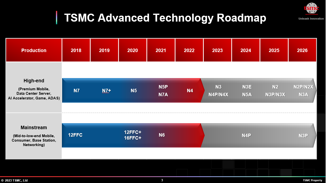
At its 2023 North American Technology Symposium today, TSMC has disclosed additional details about its plans for its forthcoming N2 2nm-class production nodes in 2025 – 2026 and beyond. TSMC's N2 family of fabrication technologies will be expanding with additional variations, including N2P with backside power delivery, and N2X for high-performance computing. Between these forthcoming N2 generation process nodes, TSMC is laying out a roadmap to continue their relentless pace of increasing transistor performance efficiency, optimize power consumption, and improving transistor density.
N2 Gets Denser
TSMC's initial N2 manufacturing process, which was introduced last year, will be the foundry's first node to use gate-all-around (GAAFET) transistors, which TSMC is calling Nanosheet transistors. GAAFET's advantages over current FinFET transistors includes lowered leakage current (as gates are present on all four sides of the channel), as well as the ability to adjust channel width for higher performance or lower power consumption.
When introducing this technology last year, TSMC said that it would enhance transistor performance by 10% to 15% with the same power and complexity, or reduce power consumption by 25% to 30% at the same clock and transistor count. The company also says that N2 will offer 'mixed' chip densities of over 15% greater than N3E, which is an increase from the 10% density increase announced last year.
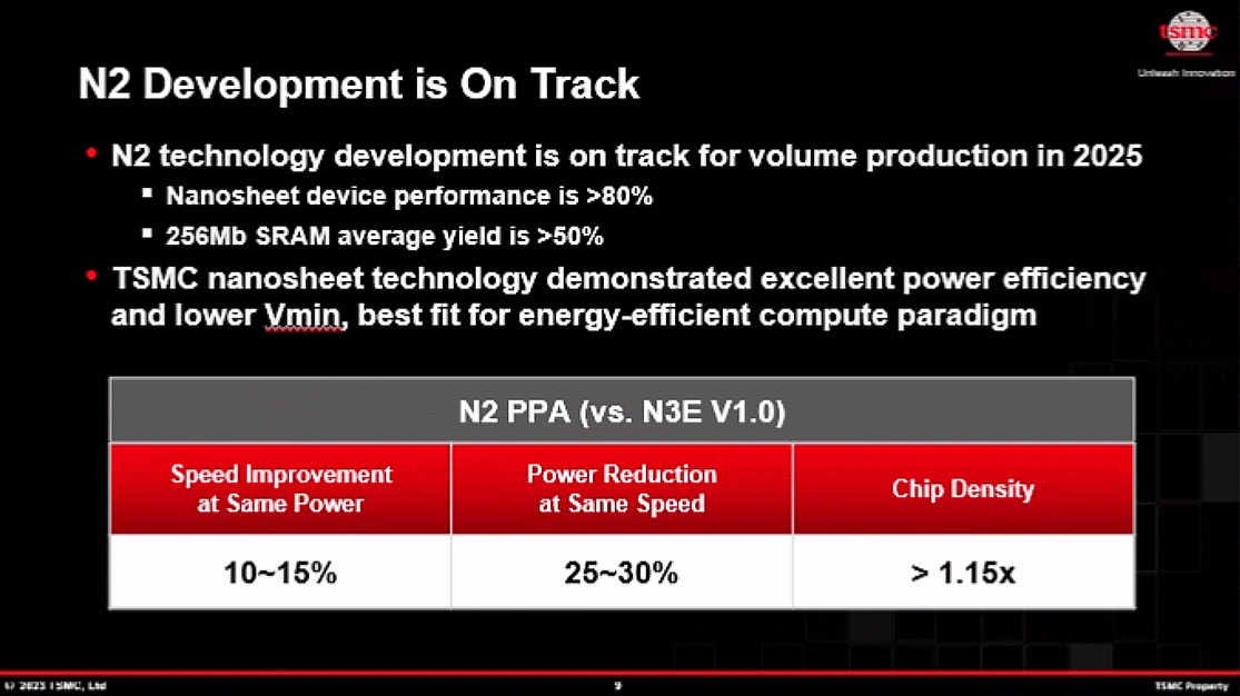
Today, the company said that N2 technology development is on track and the node will enter high-volume production in 2025 (probably very late 2025). The company also said that its Nanosheet GAA transistor performance is achieving better than 80% of its target specifications two years before entering HVM, and that average yield of a 256Mb SRAM test IC is over 50%.
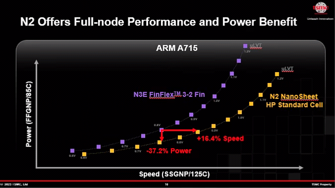
"TSMC nanosheet technology demonstrated excellent power efficiency and lower Vmin, best fit for energy-efficient compute paradigm," a statement by TSMC reads.
| Advertised PPA Improvements of New Process Technologies Data announced during conference calls, events, press briefings and press releases |
|||||
| TSMC | |||||
| N5 vs N7 |
N3 vs N5 |
N3E vs N5 |
N2 vs N3E |
||
| Power | -30% | -25-30% | -34% | -25-30% | |
| Performance | +15% | +10-15% | +18% | +10-15% | |
| Chip Density* | ? | ? | ~1.3X | >1.15X | |
| Volume Manufacturing |
Q2 2022 | H2 2022 | Q2/Q3 2023 | H2 2025 | |
*Chip density published by TSMC reflects 'mixed' chip density consisting of 50% logic, 30% SRAM, and 20% analog.
N2P Gets Backside Power Delivery In 2026
TSMC's N2 family will evolve and sometime in 2026, when the company plans to introduce its N2P fabrication technology. N2P that will add backside power rails to N2's Nanosheet GAA transistors.
Backside power delivery is meant to decouple I/O and power wiring by moving power rails to the back, addressing challenges like elevated via resistances in the back-end-of-line (BEOL). This, in turn, will enhance transistor performance and reduce their power consumption. Also, backside power deliver eliminates some potential interference between data and power connections.
Backside power delivery is innovation whose importance is hard to overstate. Chipmakers have been fighting resistances in chip power delivery circuitry for years, and backside power delivery networks (PDN) are a yet another method to address them. In addition, decoupling PDN and data connections also helps with area reduction, so expect N2P to further increase transistor density compared to N2.
For now, TSMC is not disclosing any hard numbers regarding N2P's performance, power, and area (PPA) advantages over N2. But based on what we hear from industry sources, backside power rails alone could bring a single digit power improvements and double-digit transistor density improvements.
TSMC says that N2P is on track to be production ready in 2026, so we can speculate that the first N2P-based chips will be available in 2027. This timeline would put TSMC roughly two years behind rival Intel when it comes to backside power, assuming they're able to ship their own 20A process on time in 2024.
N2X: Even More Performance
In addition to N2P, which will likely be a working horse of TSMC's 2nm generation of processes, TSMC is also prepping N2X. This will be a fabrication process tailored for high-performance computing (HPC) applications like high-end CPUs, which need increased voltages and clocks. The foundry is not outlining the specific advantages this node will compared to N2, N2P, and N3X, but as with all performance-enhanced nodes, the actual benefits are expected to depend signficantly on how much design technology co-optimization (DTCO) is practiced.


38 Comments
View All Comments
Tuna-Fish - Wednesday, April 26, 2023 - link
A fringe benefit of backside power delivery is that it will allow customers to stack less powerhungry chiplets below the more powerhungry ones without major disadvantages.Right now, AMD X3D cpus clock lower than their normal ones, partially because power dissipation is compromised because there is a cache chiplet on top of the CPU one. They cannot stack the CPU on top of the cache because they'd have to turn half of the cache chiplet into TSVs for power. If they could power the CPU chiplet from the backside, they could do that and not have to compromise.
linuxgeex - Wednesday, April 26, 2023 - link
While I get what you're thinking, it's still wrong... if you have back side power delivery and you put the cache chiplet between the power and the high-power core chiplet, that would be even more TSVs than having the power within the power chiplet and sinking data connections to the cache... and that's also missing the even bigger problem that all the IO connections would also have to go through the cache if you stuck it under the core chiplet. Putting the cache on top is still the best case. In the long term (another couple generations / years from now) the power savings will allow higher performance, since thermals are what actually limits performance. That's the lesson Intel learned with the P4, then seemed to forget until the M1 outperformed their last-gen unlocked desktop parts... now they woke up for the second time lol.Tuna-Fish - Sunday, April 30, 2023 - link
> if you have back side power delivery and you put the cache chiplet between the power and the high-power core chiplet, that would be even more TSVs than having the power within the power chiplet and sinking data connections to the cacheHow so? The only TSVs would be on the cache chiplet connecting data to the CPU. (Cache chiplet would be made on a process witthout backside power, obviously).
> the even bigger problem that all the IO connections would also have to go through the cache
This is desirable. The vast majority of the IO operations the CPU does are cached.
dotjaz - Thursday, May 11, 2023 - link
So you are basically admitting you understood nothing.The whole point is to put power lines on the opposite side of signal lines. Power hungry chips will always be below memory chips, power rail needs the shortest path to the substrate to reduce loss (that's the whole point of flip-chip packaging). All BS-PDN does is to eliminate the necessity of flip-chip and signal vias.
>How so? The only TSVs would be on the cache chiplet connecting data to the CPU
You literally know nothing.
Right now it's (bottom to top) substrate -> CCD power + signal -> CCD transistor -> 3D$ power + signal -> 3D$ transistor.
Obviously vias are required for both signal and power because CCD transistors are in the middle.
With BS-PDN (CCD only), it's (bottom to top) substrate -> CCD power -> CCD transistor -> CCD signal -> 3D$ power + signal -> 3D$ transistor.
Now only power vias are required, signal can direct bond.
YOUR PROPOSAL with BS-PDN (CCD only), it's (bottom to top) substrate 3D$ transistor -> 3D$ power + signal -> CCD power -> CCD transistor -> CCD signal
Obviously CCD power needs to face down, otherwise you'll need to use power via in the CCD itself thus completely defeat the purpose of BS-PDN, or you use wire bond - reverting to pre-FCBGA era, which is EVEN WORSE
Either way since 3D$ is entirely in the way, you need CCD power vias through 3D$ chip, you also need 3D$ power vias because 3D$ transistor is in the way, on top of that you still need signal vias since CCD power and transistor are in the way.
Let's compare with CCD BS-PDN,
**sane person** approach (3D$ on top): 3D$ power via (no signal via to substrate or 3D$, direct bonding in place)
**your proposal** (CCD on top): CCD power via + 3D$ power via + 3D$/CCD signal via + signal via to substrate
>This is desirable. The vast majority of the IO operations the CPU does are cached.
That only works if data interface is on the 3D$ like Navi31, Infinity Fabric is on the CCD not 3D$. all data must go through CCD but not 3D$. Dumbass.
dotjaz - Thursday, May 11, 2023 - link
YOUR PROPOSAL II with BS-PDN (CCD only), it's (bottom to top) substrate -> 3D$ power + signal -> 3D$ transistor -> CCD power -> CCD transistor -> CCD signal**your proposal II** (CCD on top): CCD power via + 3D$/CCD signal via (though both dies instead on just CCD) + signal via to substrate
CMOG - Wednesday, June 28, 2023 - link
Hello. Just wanted to ask an opinion on MI300 stacking GCD and CCD on top of IO. Do you think RDNA4 can use something like that? I mean put MCD below GCD so if they go with 2 GCD of let's say 80-96 CUs each the size of the package will not be massive? I have like zero knowledge on this matter that's way I'm asking you. Do you think it's possible? And if yes can it cut any cost by making the package smaller or the tech is so expensive that exceeds the smaller package savings? I would really appreciate your answer.mattbe - Friday, May 26, 2023 - link
Wish they allow upvote and downvote here. It's hilarious the person you are responding to has no idea what he was talking about and yet is still confident about it.jjjag - Monday, May 1, 2023 - link
Please don't believe for a second that anything you said was even remotely correct. Backside power just puts metal layers on both sides of the transistor. One side (front) is for local signal routing, the other side (back) is for power. This helps increase logic and routing density because you are not mixing signal wires with power, so you get more signal wires. You can do the stacking either direction -- cache on bottom or cache on top. Either way the one on bottom has to have TSVs. It's WAY less expensive to put TSVs on a cache die than it is on a CPU die. CPUs have to be produced in your best, most expensive technology, while Caches do not. Putting the CPU on top would be way better for thermal conduction. AMDs Vcache is very neat, but it's not "cool" :)Threska - Wednesday, April 26, 2023 - link
I imagine new layout tools will be needed to get the most of this technology.TeslaDomination - Wednesday, April 26, 2023 - link
I predict they’ll have even worse yield issues than their 3nm nodes.