AMD Confirms Milan-X with 768 MB L3 Cache: Coming in Q1 2022
by Dr. Ian Cutress on November 8, 2021 11:44 AM EST
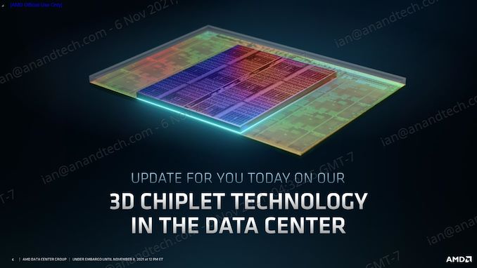
As an industry, we are slowly moving into an era where how we package the small pieces of silicon together is just as important as the silicon itself. New ways to connect all the silicon include side by side, on top of each other, and all sorts of fancy connections that help keep the benefits of chiplet designs but also taking advantage of them. Today, AMD is showcasing its next packaging uplift: stacked L3 cache on its Zen 3 chiplets, bumping each chiplet from 32 MiB to 96 MiB, however this announcement is targeting its large EPYC enterprise processors.
AMD’s current offering in this market is its third generation EPYC 7003 processor line, also known as Milan, which offers up to 64 Zen 3 cores across eight TSMC 7nm chiplets, co-packaged with a central IO die built on GlobalFoundries 14nm. The IO die provides eight DDR4-3200 memory channels and 128 lanes of PCIe 4.0, along with other things like security. Today’s announcement, or reveal (or acknowledgement?) is that coming in Q1, AMD is going to launch Milan-X.
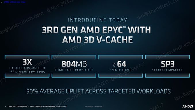
Milan-X is an upgraded version of Milan using the stacked L3 cache packaging technology. A 64-core version of Milan today, with eight 8-core chiplets, has 256 MiB of total L3 cache - the Milan-X version will use added L3 cache on each of those chiplets, creating a processor with a total 768 MiB of L3 cache, unrivalled by anything else in the industry. This extra L3 cache is built on a cache density optimized variant of TSMC N7, measures 36 mm2, and puts the added 64 MiB on top of the 32 MiB that is already there. The rest of the chiplet has a shim built around it to help with thermal transfer.
Given AMD’s disclosures about its stacked cache technology back in June at Computex, we already had been expecting consumer and enterprise variants to come to market at some point – AMD promised it would be coming to Zen 3 and put into production by the end of 2021, and this announcement today is confirming that timeline. As and when it will come to the consumer product line is still unannounced. That being said, today’s announcement is still lacking on explicit details.
AMD confirms that Milan-X will be socket compatible with current Milan processors (that’s the SP3 socket), but hasn’t listed any details about power, frequency, or pricing. We are expecting the L3 cache to consume some extra power, so if we are working to a 280 W limit, that would imply that there is some small frequency loss. Beyond that, using an effective +45% of 7nm silicon per chiplet (36mm2 for top cache, 80.7mm2 for bottom core die) should theoretically increase the price by +45% if AMD is wafer limited at TSMC and they want to keep the same cost per silicon unit area. The Milan-X actually represents a unique offering in the x86 market with so much L3 cache on offer per chiplet, so you can imagine that AMD could offer a nice premium over regular Milan.
We are told that is to come closer to launch in the first three months of next year (Q1 2022). However AMD is keen to point out that the increased cache is putting less bandwidth pressure on main memory, allowing for speedup of certain workloads by 66% (for EDA-based RTL Verification on Synopsys VCS) when comparing 16-core Milan with 16-core Milan-X, although the exact chiplet configuration was not disclosed.
AMD also went on to say that Microsoft will be announcing a public preview of their Azure HBV3 Series VMs with Milan-X today alongside AMD’s event, although didn’t talk about availability. Beyond that, the usual talk about expecting major OEM partners (Dell, Lenovo, HPE, Supermicro, Cisco) to adopt the new hardware in their portfolios at the full launch.


24 Comments
View All Comments
eSyr - Monday, November 8, 2021 - link
“we are slowly moving into an era where how we package the small pieces of silicon together is just as important as the silicon itself”—/me gives this sentence stern IBM MCM look.E. Gadsby - Monday, November 8, 2021 - link
Uh huh, because IBM has done 3D die stacking in Z right? Or did you comment without reading the article? BTW IBM has been doing MCM forever, as have others. It’s like bragging about copper interconnect at this point in time.Samus - Tuesday, November 9, 2021 - link
IBM\Motorola were first to copper interconnects. Where do you think AMD got it from :)eSyr - Monday, November 8, 2021 - link
“768 MiB of L3 cache, unrivalled by anything else in the industry”—/me gives this sentence a stern IBM z15 SC chip look.kfishy - Monday, November 8, 2021 - link
That’s an eDRAM L4 cache, the AMD announcement is about SRAM based L3 cache.saratoga4 - Monday, November 8, 2021 - link
It's not a die stack, but their eDRAM did actually stack the dram capacitor vertically below the transistors, so conceptually it's a similar idea - increase density by putting cache into the third dimension. I was always disappointed that no one else adopted the idea.Rudde - Monday, November 8, 2021 - link
How few cores could you have enabled, and still use all the 96 MB of L3 cache on a CCD?nandnandnand - Monday, November 8, 2021 - link
The answer is probably 1, as long as the software can make use of it.EPYC 72F3 has 8 chiplets with 1 core enabled on each. It would be hilarious if they made a 3D V-Cache version of that.
Kevin G - Monday, November 8, 2021 - link
96 MB of L3 cache per core would be interesting as that might be enough cache to keep a few processes/libraries fully caches while context switching between them. Schedulers would be highly incentivized to keep processes pinned as much as possible to specific cores due to how warm those caches would be.shing3232 - Monday, November 8, 2021 - link
It doesn't matter. you can use all 96M regardless