Cerebras Wafer Scale Engine News: DoE Supercomputer Gets 400,000 AI Cores
by Dr. Ian Cutress on August 21, 2020 12:00 PM EST
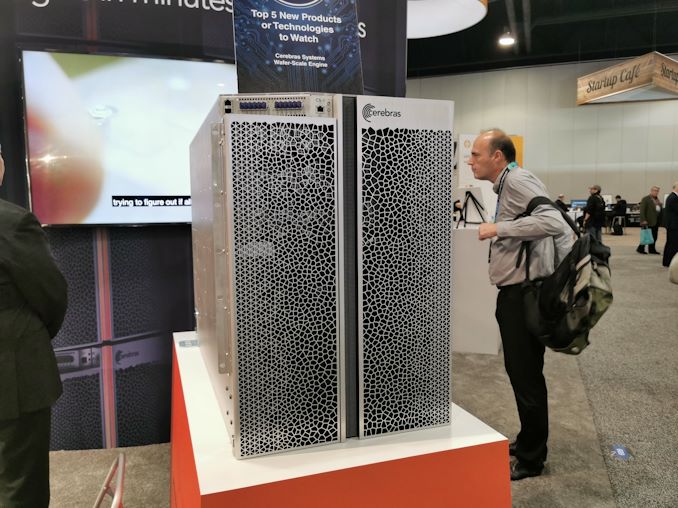
One of the more interesting AI silicon projects over the last couple of years has been the Cerebras Wafer Scale Engine, most notably for the fact that a single chip is the size of a literal wafer. Cerebras packs the WSE1 chip into a 15U custom liquid cooled server, called the CS-1, with a number of innovations regarding packaging, power, and setup. A single CS-1 requires about 20 kW of power peak, and costs around a couple million dollars (the Pittsburgh Supercomputing Center purchased two last year based on a $5m research grant). Cerebras say they have double digit customers and several dozen units already in the field, however today marks a considerable milestone as the US Department of Energy now has one deployed and working, attached directly to a supercomputer.
It is fairly easy to be marveled at Cerebras’ design, which involves a number of innovations and patents regarding cross-reticle connectivity, and the 400,000 AI cores in the processor are designed to withstand manufacturing defects by offering spare cores throughout the design that can be used in place. This gives each wafer a very good yield – every chip off the production line is useable. Cerebras is a solutions provider, not just a chip designer, and as a result it sells WSE1 in a self-contained 15U rack-mountable unit. The aim of the CS-1 design is that it can fit into any standard datacenter, you plug in the power and the networking, and away you go.
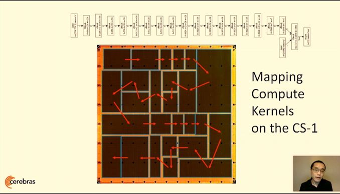
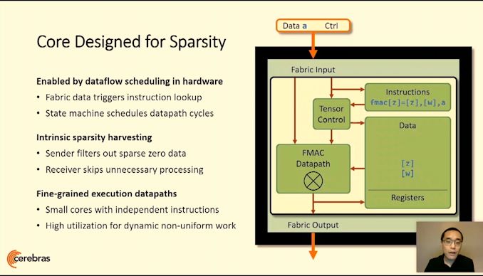
On the software side of things, Cerebras has its own graph compiler for its chip, which accepts AI networks based on TensorFlow and pyTorch, and then configures them in the most optimal way around the massive chip. This year at Hot Chips, the company went into some detail about how programming at the wafer scale works, with the compiler balancing compute and on-chip resources to use the best area-vs-performance tradeoffs for any given AI function or kernel. Each kernel can be split in model parallel or data parallel fashion in order to generate the optimal communication pattern, maximizing the performance and ultimately the on-chip use. Users can also hand-optimize kernels if required. The graph compiler is also designed to make efficient work of sparse networks, especially with having such a large chip and 18 GB of onboard SRAM as well as a full MIMD layout.
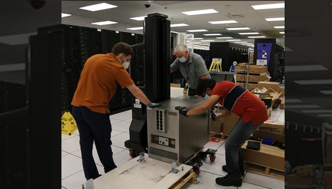
The news today however is that Cerebras is announcing a very important CS-1 installation. It may only be a single unit, but the Lawrence Livermore National Laboratory (LLNL), as funded by the US Department of Energy’s National Nuclear Security Administration, has purchased a CS-1 unit and bolted it onto its 23 PetaFLOP ‘Lassen’ Supercomputer. The Lassen supercomputer is a 684-node Power9 + Volta + Infiniband supercomputer, rated at around 23 PetaFLOPs and currently sits at #14 on the TOP500 list.
The goal of adding a CS-1 to Lassen is to help accelerate and offload targeted AI research and modelling assistance. Lassen is primarily used for nuclear simulations, material science, drug design, and medical analysis. These projects often involve longer-than-the-universe search spaces of computational analysis, and these projects are starting to use AI training and inference to help reduce the search spaces and optimize where the compute is needed, reducing wasted compute and minimizing errors. This will be one of the goals of the CS-1 attached to Lassen, both for training these search space models and then applying them at a larger scale through inference. This will be the first time that LLNL has added AI-specific hardware to its computational repertoire, and the term being used for attaching AI acceleration onto HPC compute is being called Cognitive Simulation, or CogSim for short.
“We need new answers for how to improve our ability to meet our mission requirements and to respond to ever-increasing computational requirements. Cognitive simulation is an approach that we believe could drive continued exponential capability improvements, and a system-level heterogeneous approach based on novel architectures such as the Cerebras CS-1 are an important part of achieving those improvements.” said Bronis R. de Supinski, Chief Technology Officer for Livermore Computing, who led the CS-1 procurement effort.
In discussing with Cerebras, we got an insight into how buying one of these systems works. From initial discussions to deployment to actively being used by the researchers took less than 60 days. Enabling the CS-1 through a workload manager was little more than a single line of Slurm, and users are allocated compute time on the CS-1 through a time-division multiplex queue. Currently the CS-1 cannot support multiple users simultaneously, which Cerebras told us was one of the trade-offs in getting the WSE1 to market in the time scale they have done. Future iterations are likely to work towards this goal.
As part of the sale, Cerebras and LLNL are engaging in a new AI Center of Excellence (AICoE) in order to develop and build the optimal parameters to accelerate this type of cognitive simulation into the lab workflow. Depending on the results, according to the press release, this may lead to additional Cerebras systems being attached to Lassen in the future. These could be CS-1, or potentially the new WSE2 that Cerebras teased at the end of its Hot Chips 2020 talk.
Source: LLNL, Cerebras
Related Reading
- Hot Chips 2020 Live Blog: Cerebras WSE Programming (3:00pm PT)
- 342 Transistors for Every Person In the World: Cerebras 2nd Gen Wafer Scale Engine Teased
- Cerebras’ Wafer Scale Engine Scores a Sale: $5m Buys Two for the Pittsburgh Supercomputing Center
- Hot Chips 31 Live Blogs: Cerebras' 1.2 Trillion Transistor Deep Learning Processor





6 Comments
View All Comments
kobblestown - Friday, August 21, 2020 - link
This is the coolest looking machine that I've seen in a long time.name99 - Friday, August 21, 2020 - link
"It is fairly easy to be marveled"Come on Ian! We all know the correct English is
"It is fairly easy to be emmarveled"
(Note to foreign readers. This is a joke about English that is not worth explaining if English is not your first language. Just know that NEITHER form is correct.)
abufrejoval - Saturday, August 22, 2020 - link
I am awed by the discussion, English being 3rd out of 5.FaaR - Saturday, August 22, 2020 - link
Hmm, must be one brute of a power supply, and I don't mean just the 20kW rated output capacity, when you consider that modern GPUs can have billions of transistors switching or stopping switching on timescales of thousandths of a second, that puts a lot of demand on instant power delivery.If your GPU is of the size of most of a silicon wafer on the other hand... How do they solve that? Essentially no power saving mode, burning power continuously regardless of if work is being done or not?
*shrug* Damned if I know.
IanCutress - Sunday, August 23, 2020 - link
It's actually 12x 4KW power supplies. Some redundancy built in too.Note that a Transistor has static power and active power - if its not being used for compute, active power is near zero. Also depends on the instructions. Having a cpu at 100% doing a simple loop uses less power than matrix multiplication.
PeachNCream - Sunday, August 23, 2020 - link
Neat tech! I just hope we can find a way to generate and transmit energy into these important research labs to feed their power demands without burning fossil fuels as well since energy for computation and energy for both system and facility cooling is costing us our only readily accessible, habitable place in the Universe.