Arm & TSMC Showcase 7nm Chiplet, Eight A72 at 4GHz on CoWoS Interposer
by Anton Shilov on September 27, 2019 12:40 PM EST
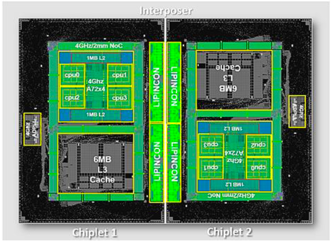
Arm and TSMC this week unveiled their jointly developed proof-of-concept chip that combines two quad-core Cortex-72-based 7 nm chiplets on TSMC’s Chip-on-Wafer-on-Substrate (CoWoS) interposer. The two chips are connected using the company’s Low-voltage-IN-Package-INterCONnect (LIPINCON) interface. The chip is meant to showcase potential of Arm’s and TSMC’s technologies for high-performance computing applications.
Large SoCs are hard and expensive to manufacture with decent yields using leading-edge process technologies these days. In fact, many elements of these SoCs do not need to be produced using the latest nodes at all. As a result, many chipmakers turn to the so-called chiplet design approach that relies on multiple smaller dies optimized for a particular function and produced using an appropriate process technology. Smaller dies afford better yields and better binning, allowing for a quicker return on investment. These smaller dies need to communicate with each other using a high-bandwidth low-latency and low-power inter-chiplet connections and the latter are the corner stone of any chiplet design.
The proof-of-concept system contains two chiplets made using TSMC’s N7 process technology and placed on a CoWoS interposer. Each chiplet features four Arm Cortex-A72 cores running at a whopping 4 GHz (this core was designed to run at <2 GHz frequencies inside mobile SoCs) that are interconnected using an on-die network-on-chip (NoC) mesh bus operating at 4 GHz. The cores are equipped with a 2 MB L2 cache (512 KB per core) as well as a 6 MB unified L3 cache.
The two chips are connected to each other using a LIPINCON die-to-die inter-chiplet connection that operates at 8 GT/s data transfer rate at 0.3 V and offers 320 GB/s bandwidth. When it comes to overall efficiency of LIPINCON on CoWoS, TSMC says that it features a 0.56 pJ/bit (pico-Joules per bit) power efficiency as well as a 1.6 Tb/s/mm2 (terabits per second per square millimeter) bandwidth density.
The proof-of-concept chiplet system was taped out in December 2018, and made in April 2019, so both Arm and TSMC had plenty of time to play with it. The chip will never be sold in volume, but it proves that technologies by the two companies can enable designers to build complex chiplet-based products with unique characteristics. THe companies are hoping that now this technology is proven that its customers will take advantage of it.
Related Reading:
- Hot Chips 31 Keynote Day 2: Dr. Phillip Wong, VP Research at TSMC (1:45pm PT)
- TSMC Announces Performance-Enhanced 7nm & 5nm Process Technologies
- TSMC: First 7nm EUV Chips Taped Out, 5nm Risk Production in Q2 2019
- TSMC Kicks Off Volume Production of 7nm Chips
Source: TSMC


26 Comments
View All Comments
jeremyshaw - Friday, September 27, 2019 - link
If I am not mistaken, this is the first 7nm A72 core. Given it's so old, my guess is this is a TSMC-lead research project, and ARM came in much later? Are than any further details on the CoWoS sandwich? Why does it have the last "oS?"name99 - Friday, September 27, 2019 - link
Chip on Wafer *on Substrate*https://en.wikichip.org/wiki/tsmc/cowos
I assume the wafer is placed on the substrate to create a package that's slightly easier to work with, the substate (I assume an organic PCB-like material) being more flexible (both mechanically, and being available as a little mini-PCB on which you can place some capacitors on inductors or whatever as required by the package)?
extide - Friday, September 27, 2019 - link
CoWoS is basically TSMC's version of an interposer.name99 - Friday, September 27, 2019 - link
Well duh.But that doesn't answer the question of why bother thinning the wafer and mounting it on substrate! That's the interesting issue, and the point I was trying to (guessing at!) answering.
anonomouse - Friday, September 27, 2019 - link
Substrate is the organic package, and it's where the technology integrates with regular packaging/mounting technologies. Plus it provides package stiffness that would definitely not exist if you tried to mount the bare interposer onto a board. And you'd still need some sort of redistribution layer from the much tighter (TSV) bumps on the backside of the interposer to a pitch that can interface with a regular motherboard.DenvR - Friday, September 27, 2019 - link
Interesting, but weird, wouldn't the A73 have been a better µarch for this project, considering the A72 was known for its high power consumption and overheating issues on mobile platforms?RSAUser - Friday, September 27, 2019 - link
It's a proof of concept, this was probably in development for a longer time.Alistair - Friday, September 27, 2019 - link
AMD style chiplet ARM CPUs incoming? Pretty neat.Raqia - Friday, September 27, 2019 - link
The A72 has a rather long 15 stage pipeline, and clock speeds like that seem more plausible for this design than A73-A77 which all have shorter pipelines. Interposers like this might be featured on the next AX chip from apple to integrate Qualcomm's modem IP which they do not have in house and can't fab on-die.Guspaz - Friday, September 27, 2019 - link
Apple bought Intel’s modem division. Why would they still be using a Qualcomm modem?