Hot Chips 2018: Xilinx 7nm ACAP Live Blog
by Ian Cutress on August 21, 2018 12:40 PM EST
12:42PM EDT - We've covered the initial announcement of Xilinx's Project Everest before, which will be coming to market as an 'ACAP' built on 7nm. Xilinx believes that the ACAP is the future of FPGA computing. The talk is set to start at 9:45am PT / 4:45pm UTC.
12:44PM EDT - Our previous coverage of the ACAP can be found here: https://www.anandtech.com/show/12509/xilinx-announces-project-everest-fpga-soc-hybrid
12:46PM EDT - Back in March, Xilinx announced Everest
12:46PM EDT - One of the key blocks is the hw/sw engine
12:46PM EDT - First time giving details
12:46PM EDT - Dev on this block has been in dev for several years
12:47PM EDT - co-designed with input from lots of groups
12:47PM EDT - Not talking about next gen product, just into the block
12:47PM EDT - Tape out in 2018
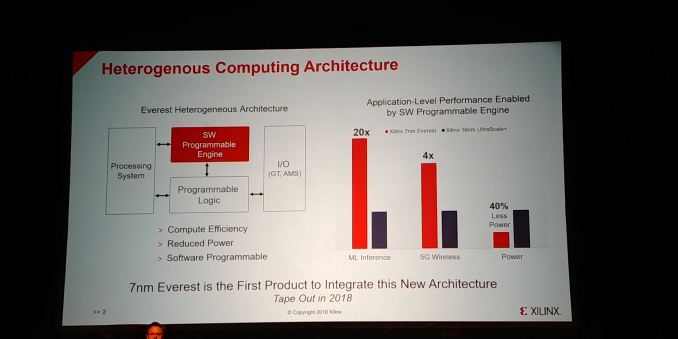
12:47PM EDT - heterogenous architecture
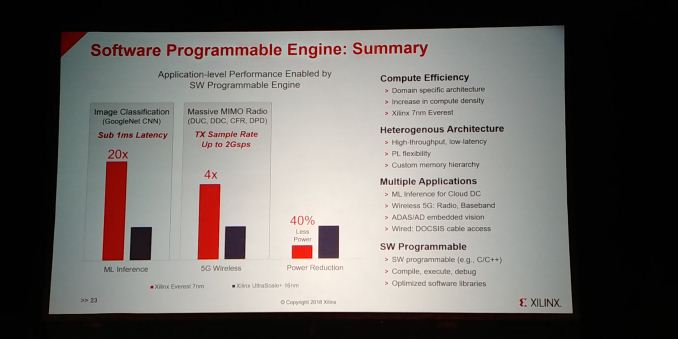
12:48PM EDT - 20x ML inference, 4x 5G wireless, 40% less power, 7nm engine vs 16nm Ultrascale FPGA
12:48PM EDT - Designed for two main benchmarks: ML Inference and 5G Wireless
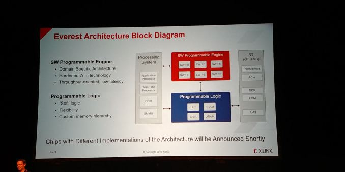
12:49PM EDT - Block diagram
12:49PM EDT - application CPU, real-time CPU
12:49PM EDT - sw engine, programmable logic with LUTs, IO
12:49PM EDT - SW Programmable Engine is a domain specific architecture, hardened in 7nm
12:49PM EDT - Scalable blog
12:49PM EDT - block
12:49PM EDT - multiple engines, can scale up
12:50PM EDT - Throughput oriented, low latency
12:50PM EDT - Targeted for ML Inference and 5G wireless
12:50PM EDT - SW Engine talks to the processing system for control
12:50PM EDT - Talks to programmable logic for high bandwidth and connectivity
12:50PM EDT - Feed the beast
12:51PM EDT - Chips with different implementations of the architecture will be announced later
12:51PM EDT - A couple of months
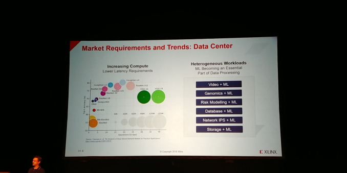
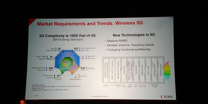
12:51PM EDT - Meeting market requirements and trends
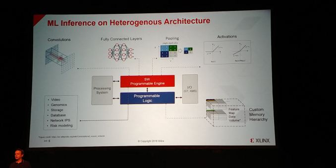
12:52PM EDT - Lots of different workloads where ML is an essential part of processing
12:52PM EDT - Can map high compute on the SW engine
12:53PM EDT - Engine and FPGA parts can work on different parts of the problem
12:53PM EDT - Processing vs data feeding
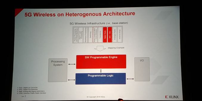
12:54PM EDT - Also 5G
12:54PM EDT - Designed to be integrated with digital radio and ADC/DAC
12:54PM EDT - Put the compute in the engine, IOs on the logic
12:54PM EDT - Control on the processor sub-system
12:54PM EDT - Now for architecture
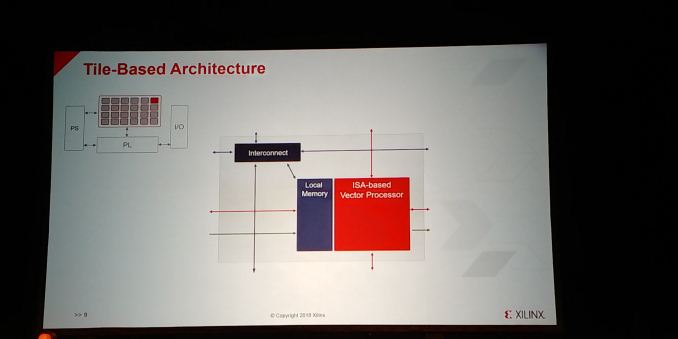
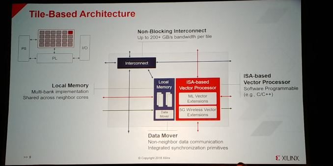
12:55PM EDT - SW Engine is Tile based Vector processor
12:55PM EDT - Each tile is interconnect, local memory, vector processor
12:55PM EDT - 100s of operations per cycle per vector processor
12:56PM EDT - Standard 2D mech interconnect with memory snooping of neighbours
12:56PM EDT - Optimized ISA for 5G and ML
12:56PM EDT - Non-blocking interconnect
12:56PM EDT - Up to 200 GB/s bw per tile
12:56PM EDT - Aggregated
12:57PM EDT - Does compute and comms in parallel
12:57PM EDT - Integrated sync of primitives
12:57PM EDT - can share partial results to next cores
12:57PM EDT - cascading interface
12:58PM EDT - Lots of individual features in other Xilinx products but put together
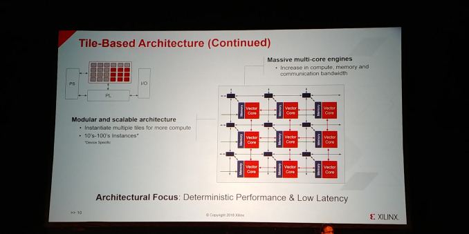
12:58PM EDT - No caches in the architecture
12:58PM EDT - Interconnect is deterministic to guarantee performance
12:58PM EDT - Massive multi-core engine
12:59PM EDT - 10-100s of tiles depending on the product
12:59PM EDT - Distributed memory heirarchy
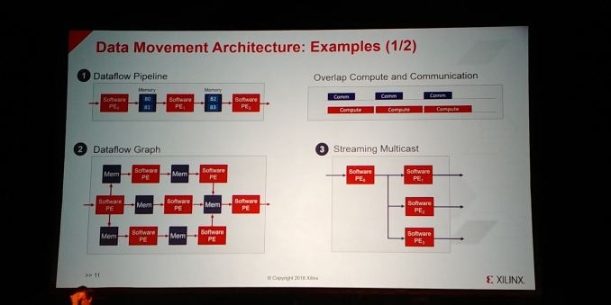
01:00PM EDT - Data flow can be pipelined or graphed
01:00PM EDT - or multicast
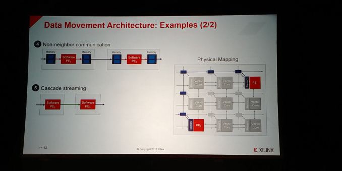
01:01PM EDT - non-neighbor communication between tiles
01:02PM EDT - through the shared memory interconnect
01:03PM EDT - Cascade streaming for dot-product
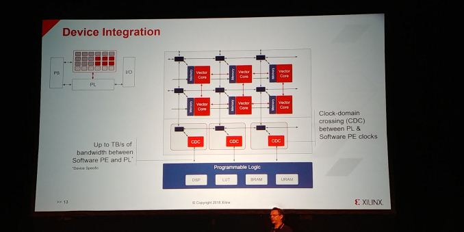
01:03PM EDT - Device integration
01:04PM EDT - with programmable logic
01:04PM EDT - Up to TB/s of bandwidth between engines and logic
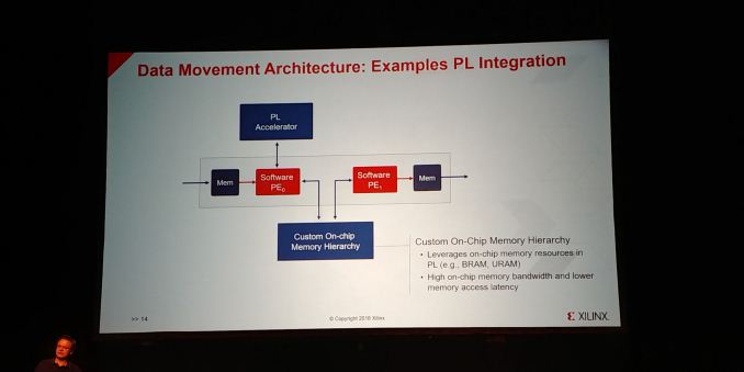
01:05PM EDT - Can include programmable accelerator
01:05PM EDT - or custom on-chip memory hierarchy
01:05PM EDT - implement specialized functions in the FPGA
01:05PM EDT - Pre/post processing or co-processing
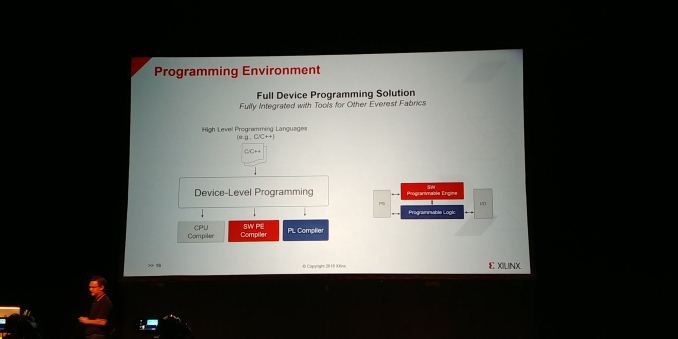
01:06PM EDT - There is going to be high-level programming languages, c/c++
01:07PM EDT - guided by the user
01:07PM EDT - Also available, one level down
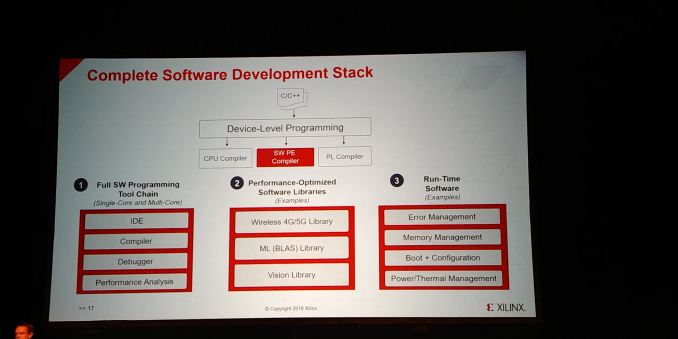
01:07PM EDT - Full SW Programming Tool Chain - IDE, COmpiler, Debugger, Perf analysis
01:08PM EDT - Performance optimized software libraries
01:08PM EDT - 4G/5G libraries, ML libraries, vision libraries
01:09PM EDT - run-time software
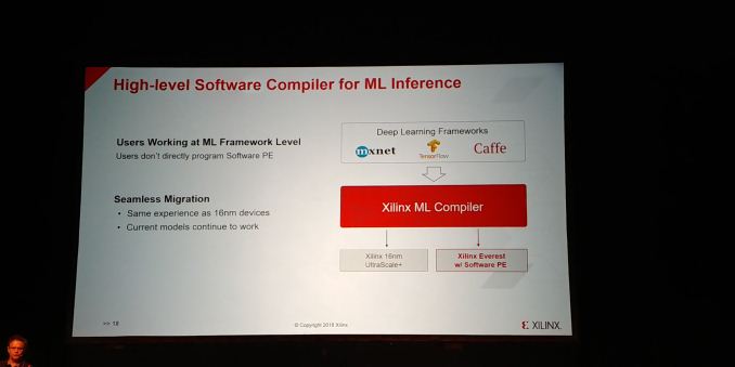
01:09PM EDT - Xilinx ML compiler on any DL framework
01:09PM EDT - Users work at framework level, compiler does it
01:09PM EDT - Seemless migration from 16nm models
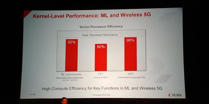
01:10PM EDT - High compute efficiency in benchmarks
01:10PM EDT - Image classification 20x over 16nm Ultrascale+
01:11PM EDT - Sub 1ms latency
01:13PM EDT - More details in the keynote later
01:13PM EDT - Xilinx Dev Forum in October
01:13PM EDT - Time for Q&A
01:14PM EDT - Q: What freq on coarse grained blocks? A: Can't tell you, but 2 Gigasamples/sec. Can't disclose power, area, frequency
01:14PM EDT - Q: What's the word-size? A: Can't disclose
01:16PM EDT - Q: Is the PE a fixed point or floating point? A: FP as well with complex math support and multiple precision support. All your favourite for ML
01:18PM EDT - Q: Does the compiler auto-vectorize, or do users write intrinsics? A: No vectorizing compiler, we do different things on that front
01:18PM EDT - That's a wrap. Time for a break, then it's Nanotube DRAM time in 30 mins.





3 Comments
View All Comments
evancox10 - Tuesday, August 21, 2018 - link
So, it's a computer oriented GPU with a NoC (network-on-chip) for data movement. "massively multicore vector ISA" == gpuevancox10 - Tuesday, August 21, 2018 - link
computer -> computekfishy - Monday, August 27, 2018 - link
This seems more generalized than a GPU though just from the interconnect along: GPUs are optimized for maximum throughput whereas the individual vector processors here appear to be more autonomous than, say, NVIDIA's CUDA cores or AMD's NCUs.