Intel Outs Z390 & X399 PCHs for Cannon Lake & Coffee Lake CPUs
by Anton Shilov on April 26, 2018 5:00 PM EST
Intel this week released its new Rapid Storage Technologies drivers, and thanks to their associated release notes, Intel has indirectly confirmed their upcoming Z390 and X399 PCHs. The drivers' release notes also shed some light on Intel’s 9th Generation Core processors as well as features of Intel’s future HEDT platform.
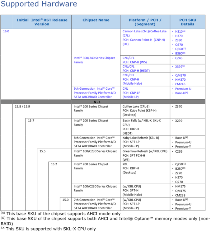
Intel’s new and upcoming platforms for desktops and workstations rely on the company’s Cannon Point-H (CNP-H) PCH silicon in various configurations and with various differentiators, according to release notes for the Intel RST version 16.0 driver. The CNP-H chip itself is already in high volume production and is sold to PC makers under the CM246, HM370, QM370, H370, H310, Q370, and B360 SKUs. Said chipsets power high-performance laptops based on mobile Coffee Lake processors as well as new motherboards for consumer and corporate desktops. Going forward, Intel’s Cannon Point-H PCH will also be used for various desktops (under the Z390, H310, H370, Q370, Q360, B360 model numbers), workstations (under the C246 model number), and high-end desktops (under the X399 SKU).
It is noteworthy that the Intel X399 PCH will be validated only with the Skylake-X CPUs (at least initially), leaving the unusual Kaby Lake-X family notably absent. It remains to be seen whether Intel plans to rebrand Skylake-X processors for the X399 platform in a bid to emphasize possible new features of the platform, but typically the company does not do anything like this in the HEDT segment.
Intel’s upcoming low-power laptop platforms running the 9th Generation Core "Cannon Lake-U" SoCs will use a different PCH known as the Cannon Point-LP. The document does not say anything about usage of non-Cannon Lake silicon in the 9th Gen Core family for low-power notebooks, so it looks like the said platforms will rely solely on Intel’s CPUs made using its 10 nm process technology. At the same time, it is also noteworthy that Intel does not list any Cannon Lake-Y SoCs in the release notes, so the destiny of such products remains unknown.
| Intel's 300-Series and 240-Series PCHs | ||||
| Chipset SKU | Silicon | Supported CPUs | Application | |
| Z390 | Cannon Point-H CNP-H |
Cannon Lake Coffee Lake-S |
Enthusiast Desktops | |
| H370 | Desktops | |||
| H310 | ||||
| Q370 | ||||
| Q360 | ||||
| B360 | ||||
| C246 | Workstations | |||
| CM246 | Cannon Lake Coffee Lake-H |
Mobile Workstations | ||
| QM370 | High-End Laptops | |||
| HM370 | ||||
| X399 | Skylake-X | High-End Desktops | ||
| 9th Gen Core Platform I/O Controller | Cannon Point-LP CNP-LP |
Cannon Point-U | Low-Power Laptops | |
Since release notes for the drivers are not meant to announce precise product specifications, it is impossible to say what exactly to expect from the Z390 or the X399 PCHs. Meanwhile, general specs of the Q370, H370 SKUs and other PCHs based on the CNP-H silicon are well known, so the base functionality of the upcoming chipsets is more or less obvious
| Intel's 300-series PCH | |||||
| Z370 | H370 | Q370 | B360 | H310 | |
| Launch | Oct '17 | Apr '18 | Apr '18 | Apr '18 | Apr '18 |
| Market | Consumer - |
Consumer Corporate |
- Corporate |
Consumer Corporate |
Consumer - |
| ME Firmware | 11 | 12 | 12 | 12 | 12 |
| HSIO Lanes | 30 | 30 | 30 | 24 | 14 |
| Total USB | 14 | 14 | 14 | 12 | 10 |
| Max USB 3.1 G2 | - | 4 | 6 | 4 | 0 |
| Max USB 3.1 G1 | 10 | 10 | 8 | 6 | 4 |
| SATA 6 Gbps | 6 | 6 | 6 | 6 | 4 |
| PCH PCIe 3.0 Lanes | 24 | 20 | 24 | 12 | - |
| PCH PCIe 2.0 Lanes | - | - | - | - | 6 |
| Max RST PCIe Storage | 3 | 2 | 3 | 1 | 0 |
| Supports Optane | Y | Y | Y | Y | N |
| Integrated 802.11ac | N | Y | Y | Y | Y |
| Intel Smart Sound | Y | Y | Y | Y | N |
| Intel vPro | N | N | Y | N | N |
| TDP | 6 W | 6 W | 6 W | 6 W | 6 W |
Intel does not comment on unreleased products, so we cannot get you any official information at this point.
Related Reading:
- Intel's 10nm Briefly Appears: Dual Core Cannon Lake in Official Documents
- Intel Documents Point to AVX-512 Support for Cannon Lake Consumer CPUs
- Intel Officially Reveals Post-8th Generation Core Architecture Code Name: Ice Lake, Built on 10nm+
- Intel 8th Generation and 9th Generation Processor Lists Leaked: Coffee Lake Refresh?
Source: Intel


25 Comments
View All Comments
jjj - Thursday, April 26, 2018 - link
Is Cannon Lake alive though? Intel confirmed today that 10nm was pushed to 2019 so got to wonder if they don't skip Cannon Lake.jjj - Thursday, April 26, 2018 - link
Intel also confirmed Whiskey Lake this year in client.HStewart - Thursday, April 26, 2018 - link
To me this sounds like Canon Lake is coming this year and not just low power cpus - but in higher end modelsjjj - Friday, April 27, 2018 - link
Cannon Lake is on 10nm and 10nm has been delayed to 2019, Intel wouldn't even say if first half or second half.edzieba - Monday, April 30, 2018 - link
10nm VOLUME is delayed due to yield issues. That doesn't rule out low volume shipping such as very small dies (e.g. the Cannon Lake 2+0 dies that shipped last year), or very high margin big dies (as Nvidia did with GP100 and GV100).Duncan Macdonald - Thursday, April 26, 2018 - link
The name is an invitation to confusion as AMD already have an X399 chipset for their Threadripper processors. I know that Intel and AMD are competitors but is a little bit of courtesy like not using the same name for chipsets too much to ask for.plopke - Thursday, April 26, 2018 - link
;p they did change the usual B350 to B360 at least , but you could argue1)keep naming scheme that they always used
2)rename everything because AMD renamed all their chips in almost the same way as intel but one version ahead
cosmotic - Thursday, April 26, 2018 - link
I would place the blame on AMD here. X399 is clearly within the established Intel X series pattern; they likely tried to make it look like they were ahead of Intel on the 'same technology'. What a nefarious move on AMD's part.Samus - Thursday, April 26, 2018 - link
True. AMD has been hijacking GPU, CPU, and now recently chipset series designations from the competition for awhile.I get there are only so many ways you can series a product. But ever since the GCN R7/R9 series starting at 2xx, they've effectively taken the space once occupied by nVidia (for better or worse) and I still laugh when I see 480 and 580 because to the older crowd, those series designations are grossly dated. It really wouldn't be that hard to do what Sony does with the Xperia phones and just have RX1, RX3, RX5, etc. Then next generation RZ1, RZ3, RZ5, etc. Then next generation RZ1+, RZ3+, RZ5+, etc. Endless possibilities, uniquely different, no confusion or comical throwbacks to nearly 10 year old GPU's.
The CPU and chipset game could have also been set uniquely apart from Intel. First of all, the name Ryzen sucks. It's just downright dumb. AMD should have stuck with their roots and used the names Athlon and even Duron for the iGPU models with Vega graphics. Their overall CPU naming scheme has been terrible since the Phenom debut and as someone who works in IT it's torture to talk to normal people about this.
The chipsets shouldn't even be chipsets; it should be identified by it's socket, then the features of the chipset. B350 boards could simply be called AM4B, X390 boards couldn't simply be called AM4X, and the 4xx series could just be called AM4B+, AM4X+, and so on. For the inevitable 6xx series (because AMD isn't going to listen to me and take all of this good, free advice I'm writing here) they could just make a new socket (which they will probably have too when they go to 7nm because the associated voltage drop will require substantially different routing and they are likely to need more pins for the increase in interconnects) they would repeat the process with AM5B, AM5X, and so on.
This is all so easy to clean up. Don't even get me started on why they decided to call the Ryzen 2nd gen CPU's 2xxx series instead of 1xxx series when they aren't really 2nd gen parts, just a refresh. Granted Intel is guilty as hell of this too (exactly how many 5th Gen Core parts were even made, ESPECIALLY on the desktop platform!) The process and manufacturing changes should just have a + or a 4th digit change, is i5-4305U instead of the i5-5300U, because the times they do this only seem to identify Crystalwell GPU's and that was really dumb...now at least they (Intel) get's it and uses a G to designate a performance GPU in the GPU.
Ugg. Marketing fails.
Ket_MANIAC - Friday, April 27, 2018 - link
You know, there is not one bit of credibility in all the stuff that you wrote, except maybe the GPU part. Who said AMD's gonna change sockets? What part of 2020 do you not understand? Granted Ryzen looks like its name was chosen by Lisa Su's daughter and Threadripper by a hormonal teen but they have done their part. As for your AM4B and AM4X naming schemes, they are limited to just 2 generations. What about the 3rd cycle of chipsets? AM4-? 4th? AM4*? Are we going full retard with arithmetic? And who said chipset names were governed by their sockets? Your own logic is flawed to the ground. You say Ryzen 2nd gen products, yet you have an issue with the 2000 naming scheme. This is CPU 2nd gen, not architecture 2nd gen. AMD isn't using names like Sandy Bridge for arch and Ivy for improvement and I think no one really has any issue with it unless you go about looking for it.And of all the companies you could have taken support of for stupid naming schemes, you come to Intel? Lol God! I will refrain from saying anything because with all due respect sir, you clearly are not familiar with anything Intel except for maybe the "Bridge" or "Lake" in you desktop and a "U" series processor with an "iGPU" in your laptop. And I am happy for you. May you never get lost in Intel's "fantastic" and "transparent as GPP" naming scheme.