The Qualcomm Snapdragon X Architecture Deep Dive: Getting To Know Oryon and Adreno X1
by Ryan Smith on June 13, 2024 9:00 AM ESTOryon CPU Architecture: One Well-Engineered Core For All
For our architectural deep dive, we’ll start with the star of the show: the Oryon CPU core.
As a quick refresher, Oryon is essentially a third-party acquisition by Qualcomm. The CPU core began life as “Phoenix”, and was being developed by the chip startup NUVIA. Comprised of numerous ex-Apple staffers and other industry veterans, NUVIA’s initial plan was to develop a new server CPU core, the likes of which would compete with the cores in modern Xeon, EPYC, and Arm Neoverse V CPUs.
However, seizing the opportunity to acquire a talented CPU development team, Qualcomm purchased NUVIA in 2021. And Phoenix was re-tasked for use in consumer hardware, reborn as the Oryon CPU core.
And while Qualcomm isn’t focusing too much on Oryon’s roots, it’s clear that the first-generation architecture – employing Arm’s v8.7-A ISA – is still deeply rooted in those initial Phoenix designs. Phoenix itself was already intended to be scalable and power efficient, so this is not by any means a bad thing for Qualcomm. But it does mean that there are a number of client-focused core design changes which didn’t make it into the initial Oryon design, and that we should expect to see in future generations of the CPU architecture.
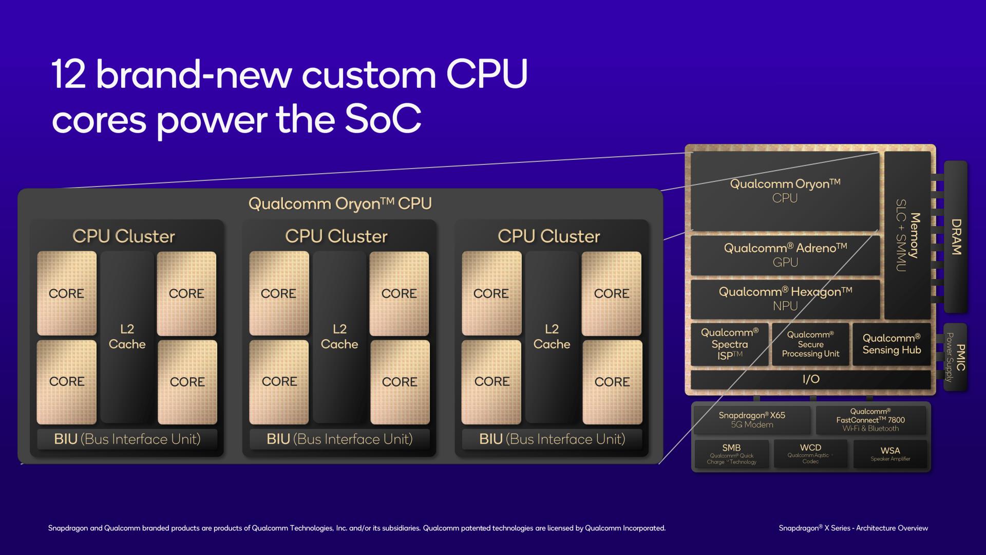
Diving in, as previously disclosed by Qualcomm, the Snapdragon X uses three clusters of Oryon CPU cores. At a high level, Oryon is designed to be a full-scale CPU core, capable of delivering both energy efficiency and performance. And to that end, it’s the only CPU core that Qualcomm needs; there aren’t separate performance-optimized and efficiency-optimized cores like there are on Qualcomm’s previous Snapdragon 8cx chips, or Intel/AMD’s most recent mobile chips, for that matter.
As far as Qualcomm is disclosing, all of the clusters are equal as well. So there isn’t an “efficiency” cluster that’s tuned for power efficiency over clockspeeds, for example. Still, only 2 CPU cores (in different clusters) can hit any given SKU’s top turbo boost speeds; the rest of the cores top out at the chip’s all-core turbo.
Each cluster, in turn, has its own PLL, so each cluster can be individually clocked and powered on. In practice this means that two of the clusters can be put to sleep during light workloads, and then roused from their sleep when more performance is needed.
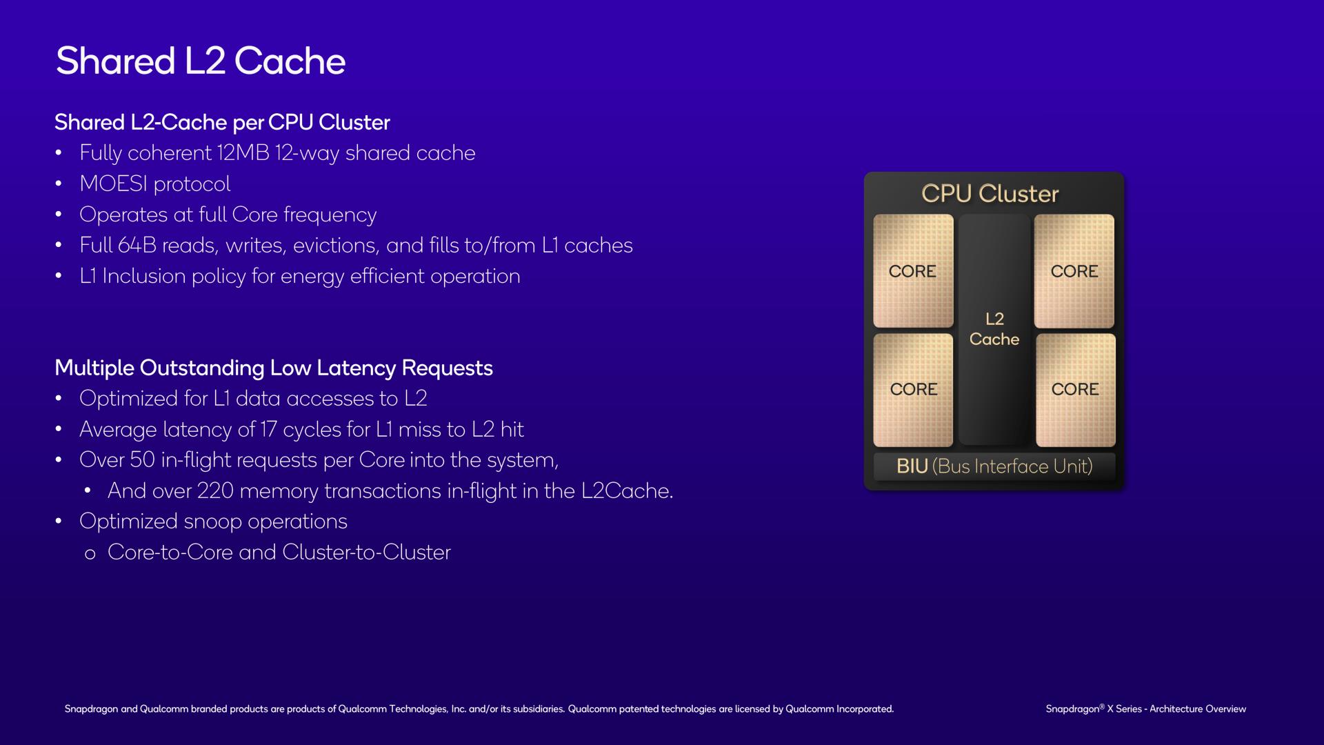
Unlike most CPU designs, Qualcomm is going with a slightly flatter cache hierarchy for Snapdragon X and the Oryon CPU core clusters. Rather than having a per-core L2 cache, the L2 cache is shared per 4 cores (this being very similar to how Intel shares the L2 cache on its E-core clusters). And this is a rather huge L2 cache, as well, at 12MB in size. The L2 cache is 12-way associative, and even with its large size, there’s only a 17 cycle latency to access the L2 cache after an L1 miss.
This is an inclusive cache design, so it contains a mirror of what’s in the L1 cache as well. According to Qualcomm they’re using an inclusive cache for energy efficiency reasons; an inclusive cache means that eviction is much simpler, as L1 data doesn’t need to be moved to L2 to be evicted (or removed from L2 when being promoted to L1). Cache coherency, in turn, is maintained using the MOESI protocol.
The L2 cache itself runs at the full core frequency. L1/L2 cache operations, in turn, are full 64 byte operations, which amounts to hundreds of gigabytes per second of bandwidth between the cache and CPU cores. And while the L2 cache is mostly in place to service its own, directly-attached CPU cores, Qualcomm has implemented optimized cluster-to-cluster snooping operations as well, for when one cluster needs to read out of another.
Interestingly, the Snapdragon X’s 4 core cluster configuration is not even as big as an Oryon CPU cluster can go. According to Qualcomm’s engineers, the cluster design actually has all the accommodations and bandwidth to handle an 8 core configuration, no doubt harking back to its roots as a server processor. In the case of a consumer processor, multiple smaller clusters offers more granularity for power management and as a better fundamental building block for making lower-end chips (e.g. Snapdragon mobile SoCs). But it will come with some trade-offs, with slower core-to-core communication when those cores are in separate clusters (and thus having to go over the bus interface unit to reach another core). It’s a small but notable distinction, since both Intel and AMD’s current designs place 6 to 8 CPU performance cores inside the same cluster/CCX/ring.
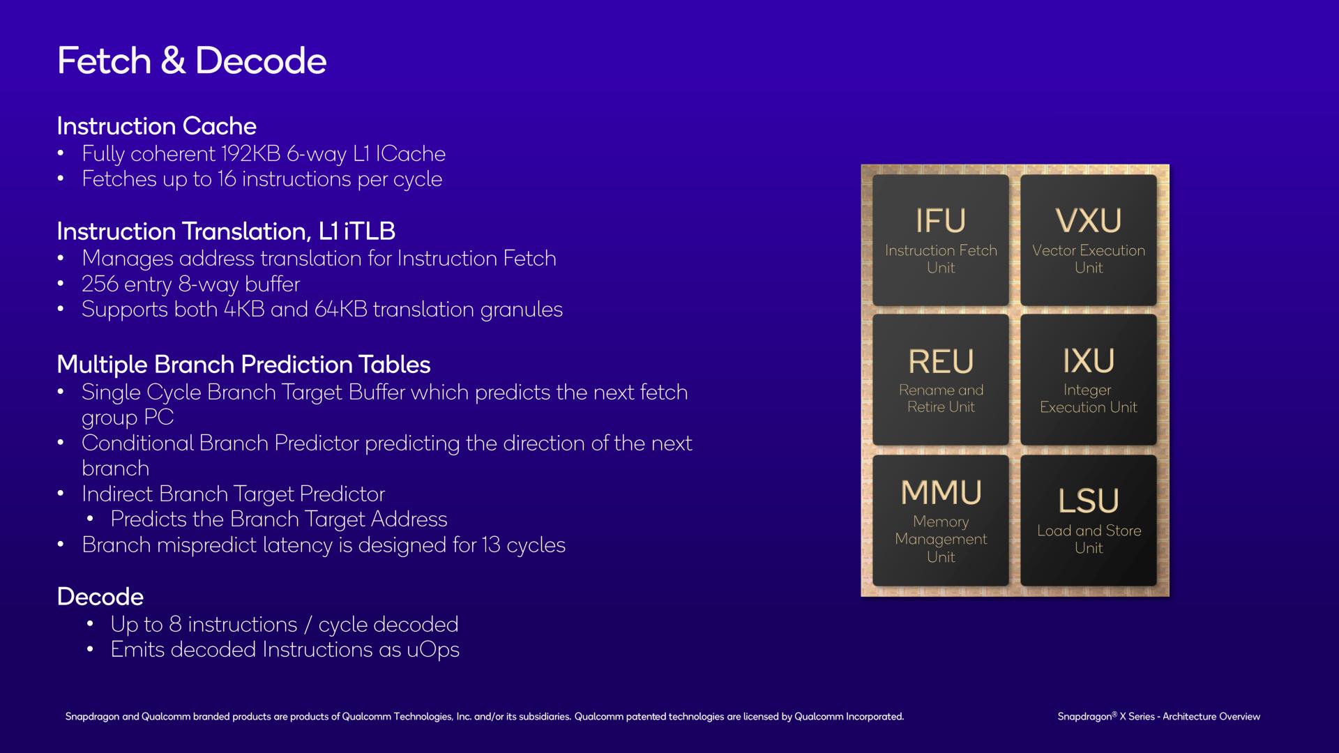
Diving into an individual Oryon CPU core, we quickly see why Qualcomm has gone with a shared L2 cache: the L1 instruction cache in a single core is already massive. Oryon ships with a 192KB L1 I-Cache, three-times the size of the Redwood Cove (Meteor Lake) L1 I-Cache, and even larger still than Zen 4’s. Overall, the 6-way associative cache allows Oryon to keep a lot of instructions very local to the CPU’s execution units. Though unfortunately, we don’t have the L1I latency on-hand to see how it compares to other chips.
Altogether, the fetch/L1 unit of Oryon can retrieve up to 16 instructions per cycle.
That, in turn, feeds a very wide decode front-end. Oryon can decode up to 8 instructions in a single clock cycle, an even wider decode front-end than Redwood Cove (6) and Zen 4 (4). And all of the decoders are identical (symmetrical), so there are no special cases/scenarios required to achieve full throughput.
As with other contemporary processors, these decoded instructions are emitted as micro-ops (uOps), for further processing by the CPU core. Each Arm instruction can technically decode for up to 7 uOps, but according to Qualcomm, Arm v8 in general tends to be much closer to a 1-to-1 ratio of instructions-to-decoded micro-ops.
Branch prediction is another major driver of CPU core performance, and this is another area where Oryon doesn’t skimp. Oryon features all the usual predictors: direct, conditional, and indirect The direct predictor is single-cycle; meanwhile, a branch mispredict carries a 13 cycle latency penalty. Unfortunately, Qualcomm is not disclosing the size of the branch target buffers themselves, so we don’t have a good idea of just how big those are.
We do, however, have the size of the L1 translation lookaside buffer (TLB), which is used for virtual-to-physical memory address mapping. That buffer holds 256 entries, supporting both 4K and 64KB pages.
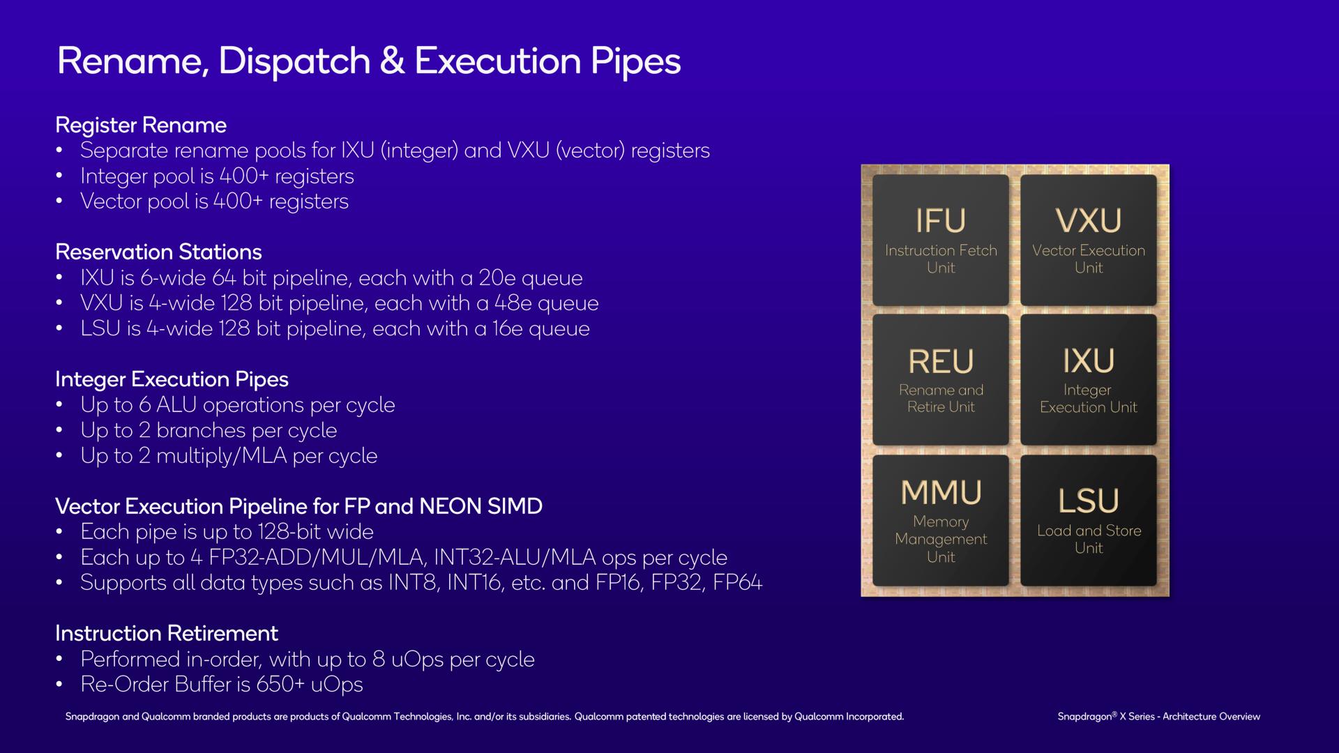
Flipping over to the execution backend of Oryon, there’s a lot to talk about. In part because there’s a lot of hardware and a lot of buffers here. Oryon features a sizeable 650+ re-order buffer (ROB) for extracting instruction parallelism and overall performance through out-of-order execution. This makes Qualcomm the latest CPU designer to throw traditional wisdom out the window and ship a massive ROB, eschewing claims that larger ROBs deliver diminishing returns.
Instruction retirement, in turn, matches the maximum capability of the decoder block: 8 instructions in, 8 uOps out. As noted before, the decoders can technically emit multiple uOps for a single instruction, but most often it’s going to be perfectly aligned with the instruction retirement rate.
The register rename pools on Oryon are also quite massive (are you sensing a common theme here?). Altogether there’s over 400 registers available for integers, and another 400 registers for feeding the vector units.
As for the actual execution pipes themselves, Oryon offers 6 integer pipes, 4 FP/vector pipes, and another 4 load/store pipelines. Qualcomm hasn’t provided a full mapping of each pipeline here, so we can’t run through all the possibilities and special cases. But at a high level, all of the integer pipelines can do basic ALU operations, while 2 can handle branches, and 2 can do complex multiply-accumulate (MLA) instructions. Meanwhile, we’re told that the vast majority of integer operations have a single cycle latency – that is, they execute in a single cycle.
On the floating point/vector side of things, each of the vector pipelines has its own NEON unit. As a reminder, this is an Arm v8.7 architecture, so there aren’t any vector SVE or Matrix SME pipelines here; the CPU core’s only SIMD capabilities are with classic 128-bit NEON instructions. This does limit the CPU to narrower vectors than contemporary PC CPUs (AVX2 is 256-bits wide), but it does make up for the matter somewhat with NEON units on all four FP pipes. And, since we’re now in the era of AI, the FP/vector units support all the common datatypes, right on down to INT8. The only notable omission here is BF16, a common data type for AI workloads; but for serious AI workloads, this is what the NPU is for.
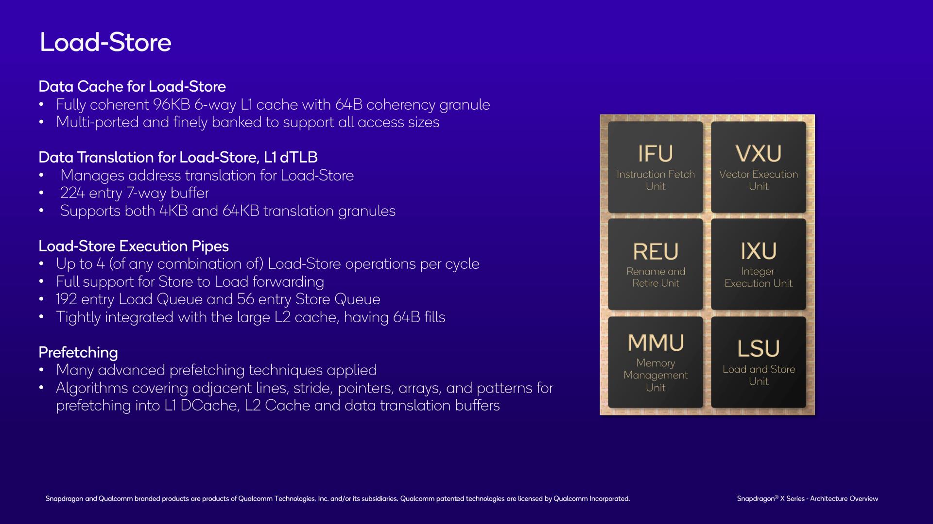
Branching off to its own slide, we have the data load/store units on Oryon. The core’s load/store units are fully flexible, meaning that the 4 execution pipes can do any combination of loads and stores per cycle as needed. The load queues themselves can go up to 192 entries deep, while the store queues can go up to 26 entries. And all fills are the full size of a cache line: 64 bytes.
The L1 data cache supporting the load/store units is also quite sizable in its own right. The fully coherent 6-way associative cache is 96KB in size, twice the size of what you’ll find on Intel’s Redwood Cove (though the upcoming Lion Cove will significantly change this). And it’s finely banked, in order to efficiently support a wide variety of different access sizes.
Otherwise, Qualcomm’s memory prefetcher wanders a bit into “secret sauce” territory, as the company says the relatively complex unit contributes a great deal to performance. Consequently, Qualcomm isn’t saying too much about how their prefetcher works, but it goes without saying that its ability to accurately predict and prefetch data can have a huge impact on the CPU core’s overall performance, especially with how long a trip is to DRAM at modern processor clockspeeds. Overall, Qualcomm’s prefetch algorithms seek to cover multiple cases, ranging from simple adjacencies and strides up to more complex patterns, using past access history to predict future data needs.
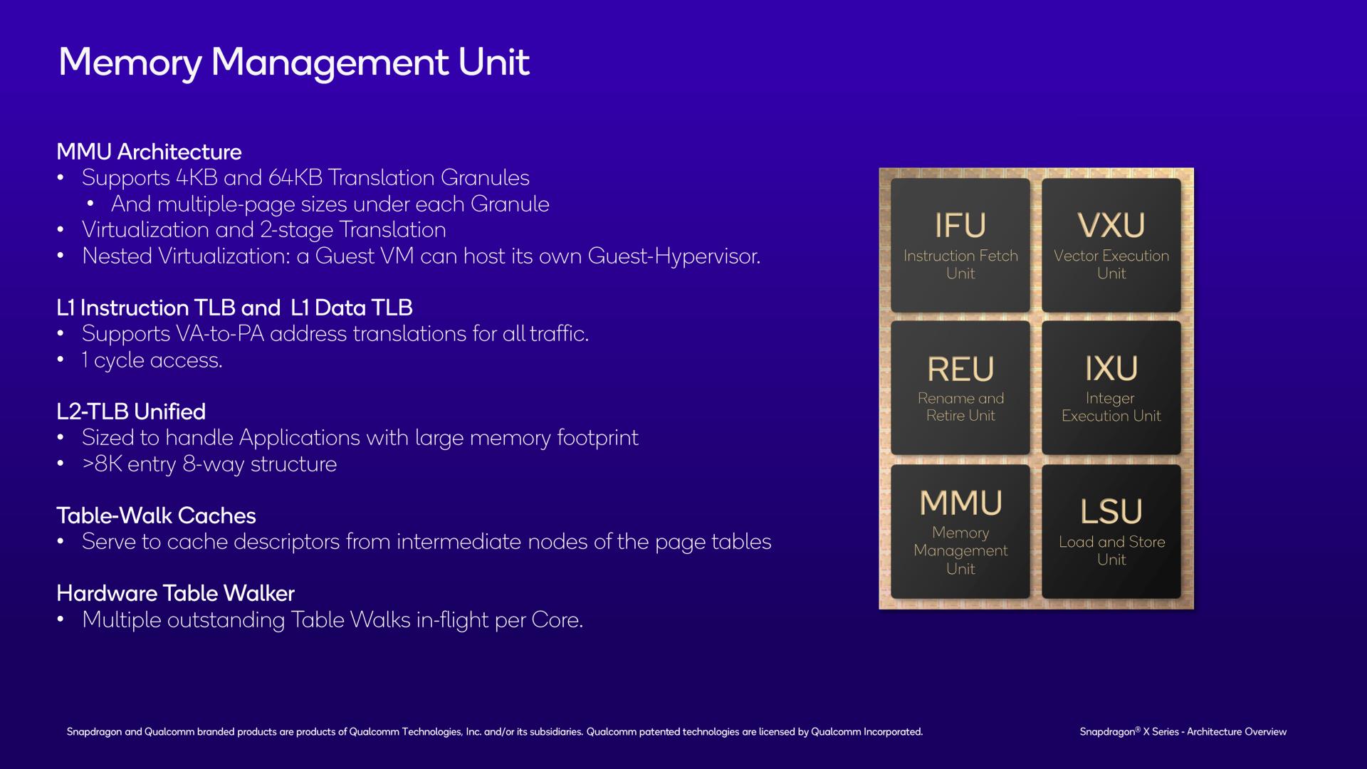
Conversely, Oryon’s memory management unit is relatively straightforward. This is a fully-featured, modern MMU, and it supports even more esoteric features such as nested virtualization – which allows a guest virtual machine to host its own guest hypervisor for even more virtual machines farther down.
Of other notable capabilities here, the hardware table walker is another special mention. The unit, responsible for going out to DRAM if a cache line isn’t in either the L1 or L2 caches, supports up to 16 concurrent table walks. And keep in mind this is per core, so a complete Snapdragon X chip can be doing upwards of 192 table walks at a time.
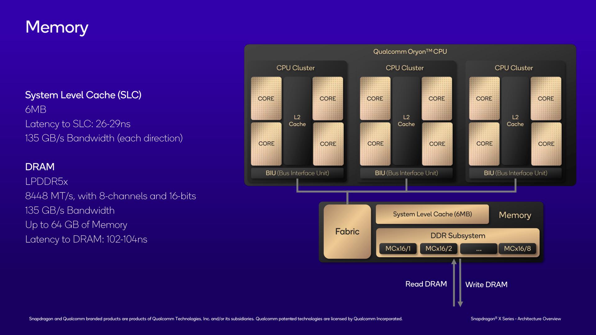
Finally, going beyond the CPU cores and the CPU clusters, we have the highest level of the SoC: the shared memory subsystem.
It’s here where the final level of cache resides, with the chip’s shared L3 cache. Given how big the L1 and L2 caches are for the chip, you might think that the L3 cache would also be quite sizeable. And you’d be wrong. Instead, Qualcomm has outfit the chip with just 6MB of L3 cache, a fraction of the size of the 36MB of L2 cache that it’s backstopping.
With the chip already being cache-heavy at the L1/L2 level, and with the tight integration between those caches, Qualcomm has gone with a relatively small victim cache here to serve as the last stop before going out to system memory. Coming from traditional x86 CPUs, it’s quite a significant change, though it’s very on-brand for Qualcomm, whose Arm mobile SoCs also normally feature relatively small L3 caches. The upside, at least, is that the L3 cache is quite quick to access, at only 26-29 nanoseconds of latency. And it has the same amount of bandwidth as the DRAM (135GB/sec) to pass data between the L2 cache below it and the DRAM above it.
As for memory support, as noted in previous disclosures, Snapdragon X features a 128-bit memory bus with LPDDR5X-8448 support, giving it a maximum memory bandwidth of 135GB/second. At current LPDDR5X capacities, this allows Snapdragon X to address up to 64GB of RAM, though I wouldn’t be too surprised down the line if Qualcomm validates it for 128GB once higher density LPDDR5X chips start shipping.
Notably, unlike some other mobile-focused chips, Snapdragon X does not use on-package memory of any kind. So LPDDR5X chips will go on the device motherboard itself, and it’s up to device vendors to choose their own memory configurations.
With LPDDR5X-8448 memory, Qualcomm tells us that DRAM latency should be just over 100ns, at 102-104ns.
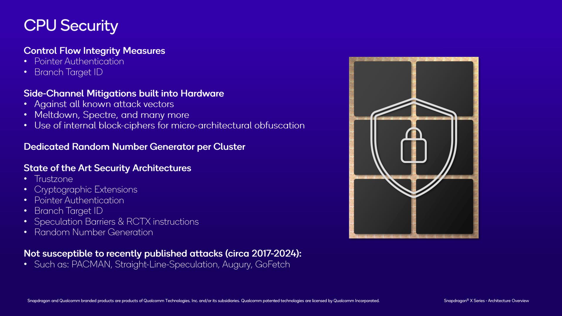
And because this is the last CPU architecture slide, we may as well throw in a quick mention of CPU security. Qualcomm supports all the security features you’d come to expect from a modern chip, including Arm TrustZone, per-cluster random number generators, and security-hardening features such as pointer authentication.
Notably, Qualcomm is claiming that Oryon has mitigations for all known side-channel attacks, including Spectre, an attack that has earned a reputation as “the gift that keeps on giving.” This is an interesting claim as Spectre isn’t really a hardware vulnerability itself, but rather is an inherent consequence of speculative execution. Which in turn is why it’s so difficult to fully defend against (and the best defense is having sensitive operations fence themselves off). None the less, Qualcomm believes that by implementing various obfuscation tools within the hardware, they can protect against these kinds of side-channel attacks. So it will be interesting to see how this plays out.
A Note on x86 Emulation
And finally, I’d like to take a moment to make a quick note on what we’ve been told about x86 emulation on Oryon.
The x86 emulation scenario for Qualcomm is quite a bit more complex than what we’ve become accustomed to on Apple devices, as no single vendor controls both the hardware and the software stacks in the Windows world. So for as much as Qualcomm can talk about their hardware, for example, they have no control over the software side of the equation – and they aren’t about to risk putting their collective foot in their mouth by speaking in Microsoft’s place. Consequently, x86 emulation on Snapdragon X devices is essentially a joint project between the two companies, with Qualcomm providing the hardware, and Microsoft providing the Prism translation layer.
But while x86 emulation is largely a software task – it’s Prism that’s doing a lot of the heavy lifting – there are still certain hardware accommodations that Arm CPU vendors can make to improve x86 performance. And Qualcomm, for its part, has made these. The Oryon CPU cores have hardware assists in place to improve x86 floating point performance. And to address what’s arguably the elephant in the room, Oryon also has hardware accommodations for x86’s unique memory store architecture – something that’s widely considered to be one of Apple’s key advancements in achieving high x86 emulation performance on their own silicon.
Still, no one should be under the impression that Qualcomm’s chips will be able to run x86 code as quickly as native chips. There’s still going to be some translation overhead (just how much depends on the workload), and performance-critical applications will still benefit from being natively compiled to AArch64. But Qualcomm is not fully at the mercy of Microsoft here, and they have made hardware accommodations to improve their x86 emulation performance.
In terms of compatibility, the biggest roadblock here is expected to be AVX2 support. Compared to the NEON units on Oryon, the x86 vector instruction set is both wider (256b versus 128b) and the instructions themselves don’t perfectly overlap. As Qualcomm puts it, AVX to NEON translation is a difficult task. Still, we know it can be done – Apple quietly added AVX2 support to their Game Porting Toolkit 2 this week – so it will be interesting to see what happens here in future generations of Oryon CPU cores. Unlike Apple’s ecosystem, x86 isn’t going away in the Windows ecosystem, so the need to translate AVX2 (and eventually AVX-512 and AVX10!) will never go away either.


51 Comments
View All Comments
Dolda2000 - Thursday, June 13, 2024 - link
I think we already knew there's no excuse for Apple not to support OpenCL and Vulkan. It's funny how Apple turned from being a supporter and inventor of open standards in the 2000s to "METAL ONLY" as soon as the iPhone became big. ReplyFWhitTrampoline - Thursday, June 13, 2024 - link
Imagine this, Just as Linux/MESA Gets a Proper and up to date to OpenCL(Rusticl: Implemented in the Rust Programming language) implementation to replace that way out of date and ignored for years MESA Clover OpenCL implementation, the Blender Foundation not a year or so before that goes on and Drops OpenCL as the GPU compute API in favor of CUDA/PTX and so there goes Radeon GPU compute API support over to ROCm/HIP that's needed to take that CUDA(PTX Intermediate Language representation) and convert/translate that to a form that can be executed on Radeon GPUs. And ROCm/HIP is never really been for consumer dGPUs or iGPUs and Polaris graphics was dropped from the ROCm/HIP support matrix years ago and Vega graphics is ready to be dropped as well! And so that's really fragmented the GPU compute API landscape there as Blender 3D 3.0/later editions only have native back end support for Nvidia CUDA/PTX and Apple Metal. So AMD has ROCm/HIP and Intel Has OneAPI that has similar functionality to AMD's ROCm/HIP. But Intel's got their OneAPI working good with Blender 3D for ARC dGPUs and ARC/Xe iGPUs on Linux as well while on Linux AMD's ROCm/HIP is not an easy thing for the non Linux neck-beard to get installed and working properly and only on a limited set of Linux Workstation Distros, unlike Intel's OneAPI and Level-0.But I'm on Zen+ and Vega 8/iGPU with a Polaris dGPU on one laptop and on Zen+ and Vega 11/iGPU on my ASRock X300 Desk Mini! And so my only hope at Blender 3D dGPU and iGPU accelerated cycles rendering is using Blender 2.93 and earlier editions that are legacy but still use OpenCL as the GPU compute API! But I'm still waiting for the Ubuntu folks to enable MESA/Rusticl instead of having that hidden behind some environment variable because that still unstable, and I'm downstream of Ubuntu on Linux Mint 21.3.
So I'm waiting for Mint 22 to get released to see if I will ever be able to get any Blender 3D iGPU or dGPU Accelerated Cycles rendering enabled because I do not want to use the fallback default and Blender's CPU accelerated Cycles rendering as that's just to slow and too stressful on the laptop and the Desk Mini(I'm using the ASRock provided cooler for that). Reply
name99 - Saturday, June 15, 2024 - link
"It's funny how Apple turned from being a supporter and inventor of open standards"You mean how Apple saw the small minds at other companies refuse to advance OpenCL and turn OpenGL into a godawful mess and concluded that trying to do things by committee was a complete waste of time?
And your solution for this is what? Every person who actually understands the issues is well aware of what a clusterfsck Vulkan is, eg https://xol.io/blah/death-to-shading-languages/
There's a reason the two GPU APIs/shading languages that don't suck (Metal and CUDA) both come from a single company, not a committee. Reply
Dante Verizon - Sunday, June 16, 2024 - link
The reason is that there are few great programmers. Replydan82 - Thursday, June 13, 2024 - link
Thanks for the write-up. I'm very much looking forward to the extra competition.I assume AVX2 emulation would be too slow with Neon. While it's possible to make it work, it would perform worse than SSE, which isn't what any application would expect. And the number of programs that outright require AVX2 are probably very few. I'm assuming Microsoft is waiting for SVE to appear on these chips before implementing AVX2 emulation. Reply
drajitshnew - Thursday, June 13, 2024 - link
Thanku Ryan and AT for a good CPU architecture update. It is a rare treat these days ReplyHulk - Thursday, June 13, 2024 - link
I think this might have been important if Lunar Lake wasn't around the corner. But after examining Lunar Lake I think this chip is overmatched. Good try though. ReplySIDtech - Friday, June 14, 2024 - link
😂😂😂😂 ReplyFWhitTrampoline - Thursday, June 13, 2024 - link
"Meanwhile the back-end is made from 6 render output units (ROPs), which can process 8 pixels per cycle each, for a total of 48 pixels/clock rendered. The render back-ends are plugged in to a local cache, as well as an important scratchpad memory that Qualcomm calls GMEM (more on this in a bit)."No that's 6 Render Back Ends of 8 ROPs each for a total of 48 ROPs and 16 more ROPs than either the Radeon 680M/780M(32 ROPs) or the Meteor Lake Xe-LPG iGPU that is 32 ROPs max. And so the G-Pixel Fill Rates there are on one slide and that is stated as 72 G-Pixels/S and really I'm impressed there with that raster performance!
Do you have the entire Slide Deck for this release as the slide I'm referencing with the Pixel fill rates as in another article or another website ? Reply
Ryan Smith - Thursday, June 13, 2024 - link
So the industry as a whole has always played a little fast and loose with how the term ROPs is thrown around. In all modern architectures, what you have is not X number of single units, but rather a smaller number of units that can render multiple pixels per cycle. In this case, 6 units, each of which can spit out 8 pixels.For historical reasons, we often just say ROPs = pixel count, and move on from there. It doesn't really harm anyone, even if's' not quite correct.
But since this is our first deep dive into the Adreno GPU architecture, I wanted to get this a bit more technically correct. Hence the wording I used in the article.
"Do you have the entire Slide Deck for this release as the slide I'm referencing with the Pixel fill rates as in another article or another website ? "
Yes, the complete slide deck is posted here: https://www.anandtech.com/Gallery/Album/9488 Reply